Diving into JTAG — Debugging (Part 2)
As noted in my previous article Diving into JTAG protocol. Part 1 — Overview, JTAG was initially developed for testing integrated circuits and printed circuit boards. However, its potential for debugging was realized over time, and now JTAG has become the standard protocol for microcontroller debugging. Many Firmware and Embedded engineers first encountered it in this particular context.
In this second part of a JTAG deep-dive series, we take an in-depth look at interacting with a microcontroller’s memory and engaging with the processor core and debug registers. While the use of JTAG in testing is fairly standardized when it comes to debugging, each processor architecture has its unique nuances. With that in mind, this article will focus on debugging using JTAG on the ARM Cortex-M architecture, specifically with the STM32F407VG microcontroller.
For successful debugging, it’s not enough to simply know the basics of JTAG. It’s also essential to understand the workings of the ARM Debug Access Port, a key component that allows access to the controller’s internal registers and memory. I’ve detailed this module in the article A Deep Dive into the ARM Debug Access Port. With that groundwork laid, let’s dive into the world of debugging through JTAG.
Table of Contents
JTAG Access to the STM32F407VG Controller
Before connecting to the STM32F407VG controller via the JTAG protocol, we need to determine the following: the length of the IR register and the number of TAP controllers connected to the JTAG chain. The official documentation, specifically the RM0090: Reference manual, can assist us in this.
According to this document, the STM32F407VG has two TAP controllers: the STM32 Boundary Scan and the CoreSight JTAG-DP. The first in the chain is the Boundary Scan TAP with a IR register size of 5 bits. Following it is the CoreSight JTAG-DP TAP with a IR register size of 4 bits.

This knowledge is crucial for us because it determines how many bits to send in the JTAG chain and in what sequence to do so when accessing different TAP controllers. According to this information, we can connect to the CoreSight JTAG-DP TAP controller and attempt to read its IDCODE.
Read of ID CODE
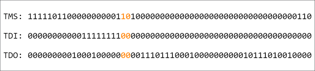
The sequence of bits for reading the IDCODE of the CoreSight JTAG-DP TAP controller will look as follows:
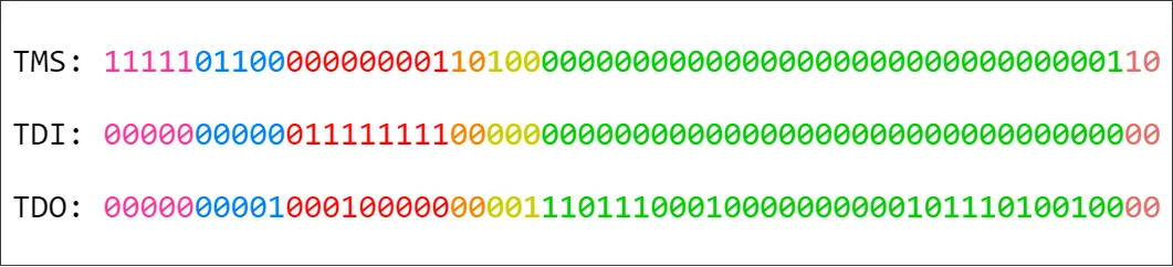
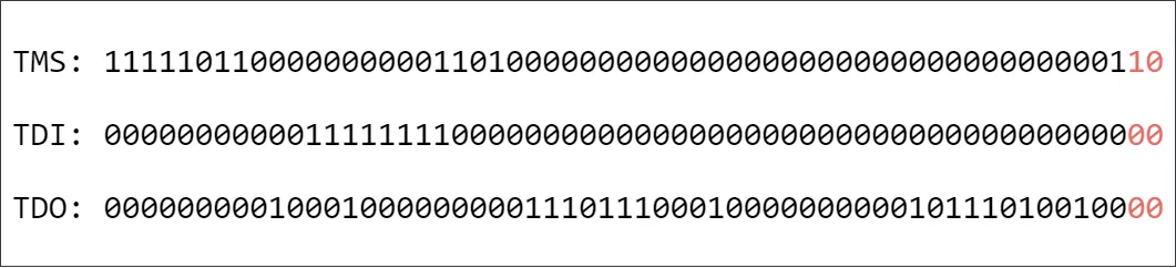
Let’s analyze this sequence in detail:
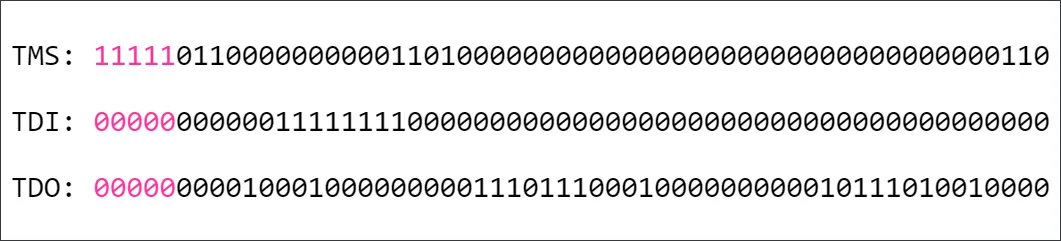
- So the first step is to reset the TAP State Machine to the initial state
Test-Logic-Resetin order to be sure that we are in a known state. To achieve this, simply hold theTMSin logic 1 for 5 clock cycles ofTCK. The pink bit sequence is responsible for this step:
- Next, we need to load the
IDCODEcommand code into theIRregister, and to do this we put the TAP State Machine into theShift-IRstate. To do this, feed theTMSline with the sequence [0, 1, 1, 0, 0]. A sequence of blue bits is responsible for this step:
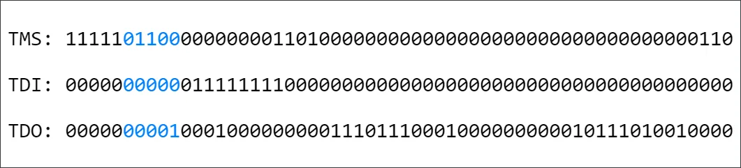
As you can see on the TDO line in the last measure there is a one. Let’s find out where it came from. The thing is that going through the Capture-IR state, the TAP controller loads into the shift register a value of 0b0001 for CoreSight JTAG-DP TAP and 0b00001 for Boundary Scan TAP which starts to move along the TDO line from this measure and LSB bits forward. So, over the next 9 clock cycles (including this one) we will get a TDO sequence of 0b100010000.
- The next step is to directly load the
IDCODEcommand code into the CoreSight JTAG-DP TAPIRregister and theBYPASScommand code into the Boundary Scan TAPIRregister. I think the situation for the CoreSight JTAG-DP TAP is clear, but why we load theBYPASScommand into the Boundary Scan TAP should be explained. You remember that there are two TAP controllers in our JTAG chain connected in series and we can not access the CoreSight JTAG-DP TAP registers without having to write something to the Boundary Scan TAP, and the size of theIRregister for Boundary Scan is 5 bits, and theDRregister is 32 bits, so to write a new data to theDRregister of the CoreSight JTAG-DP TAP we need to write a 32 + 32 = 64 bits sequence of bits to the JTAG circuit. This is not very convenient. TheBYPASScommand will help us here. When this command is in the registerIRthe data register of the selected TAP becomes 1 bit long. So now we need to write a sequence of 33 bits Instead of 64. TheIDCODEcode is0b1110, and theBYPASScommand code is0b11111total we need to push 9 bits:0b011111111. TheTMSinput must be held at logical 0 during the 8 LSB input in order for the machine to remain inShift-IRstate. The MSB bit of the instruction is pushed in when there is an exit from this state by settingTMSto logical 1. The red bit sequence is responsible for this step:
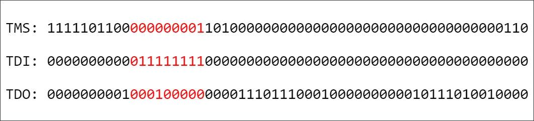
The TDO wire continues to output the sequence 0b100010000 which was loaded in the Capture-IR state.
After this step, we are in the Exit1-IR state.
- Great, the necessary commands are set in the
IRregisters and now we need to return to theRun Test/Idlestate for further work. At this point, thanks to the last 1 on theTMSline we are in theExit-1-IR stateand hence according to the state diagram we need to set the following bit sequence on theTMSline toRun Test/Idle: [1, 0]. The orange bit sequence is responsible for this step:
- After setting the
IDCODEcommand in theIRregister we need to readIDCODEfrom theDRregister. To do this the first step is to go to theShift-DRstate. To do this we set the following bit sequence [1, 0, 0] on theTMSpin considering that we are in theRun Test/Idlestate at the moment. The yellow bit sequence is responsible for this step:
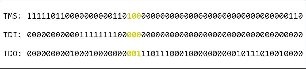
On the TDO line we have the sequence: [0, 0, 1]. The last one is already the LSB of our chip ID. The fact is that passing through the Capture-DR state our chip ID is loaded into the shift register and begins to move outward in the next clock cycles.
- In the
Shift-DRstate the remaining bits of the chip ID are unloaded. To remain in theShift-DRstate theTMSinput must be held at logic 0 during the input of all bits except the MSB bit. The MSB data is pulled out when this state is exited by settingTMSto a logical 1. The green bit sequence is responsible for this step:
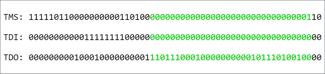
So we got a chip ID of the following kind:
11101110001000000000010111010010
Let’s check this code according to the documentation:
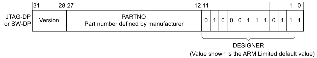
Something is wrong here. What is wrong is that the LSB is in the usual position in the figure, but we took it in the inverted order. Let’s correct this situation:
01001011101000000000010001110111
- And the final step is to go back to the
Run Test/Idlestate:
Interaction with memory
Great, the JTAG connection works and we’ve read the IDCODE. Let’s now proceed and try interacting with the microcontroller’s memory by writing a value to it and reading it back. After all, reading/writing memory is one of the primary operations when debugging a microcontroller.
To interact with the microcontroller’s memory, we need to understand the mechanism behind it. The JTAG protocol itself doesn’t provide any specifics about this. Access to the internal resources of ARM architecture controllers (such as memory) is facilitated by a special module called DAP (Debug Access Port). I’ve detailed this module extensively in this article A Deep Dive into the ARM Debug Access Port. Unfortunately, without this knowledge, advancing further might be challenging. Therefore, I highly recommend reading that article or the official documentation IHI0031 — ARM Debug Interface.
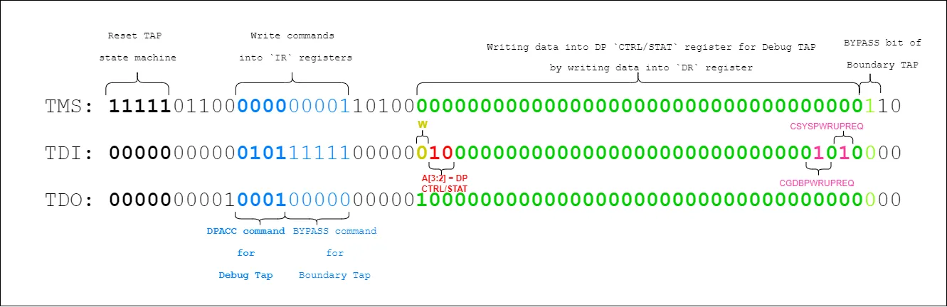
The first step for any access operation to the internal resources of an ARM architecture microcontroller with a DAP module is to request clocking and power for the debug module. This is done by setting the CSYSPWRUPREQ and CDBGPWRUPREQ bits in the DP CTRL/STAT register.
After this initial setup, we can begin our memory operations.
In the following two sections, I will be heavily referencing the “Practical Part” from the article A Deep Dive into the ARM Debug Access Port. This section describes the algorithm for reading/writing memory through interaction with the DAP module. Additionally, I will supplement this algorithm with a sequence of bits, illustrating how this will appear from the perspective of the JTAG protocol.
Writing a variable to memory
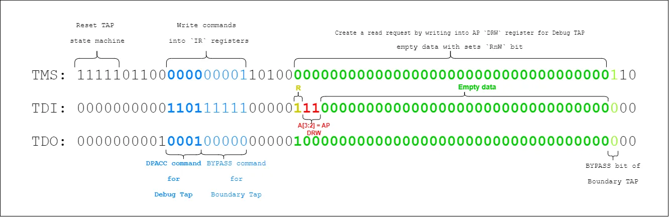
Alright, let’s write the value 0xAA55AA55 to the address 0x20000000:
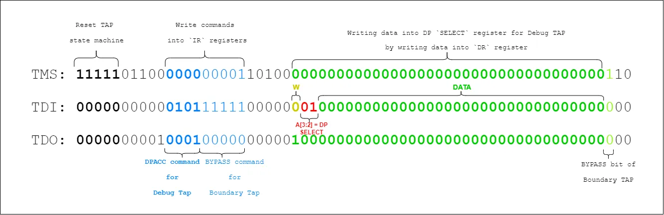
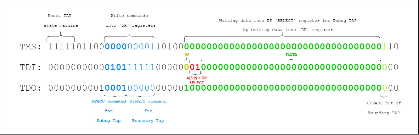
First, write 0b1010 (the DPACC register code) into the IR register. Some settings in the AP register CSW need to be configured. To access this register, we need to select the corresponding AP and register bank in the DP SELECT register. Write to the DR register:
- DATA[31:0] =
0x00 - APSEL[31:24] =
0x00 - APBANKSEL[7:4] =
0x00 - A[3:2] =
0b10(address ofSELECTregister) - RnW =
0b0
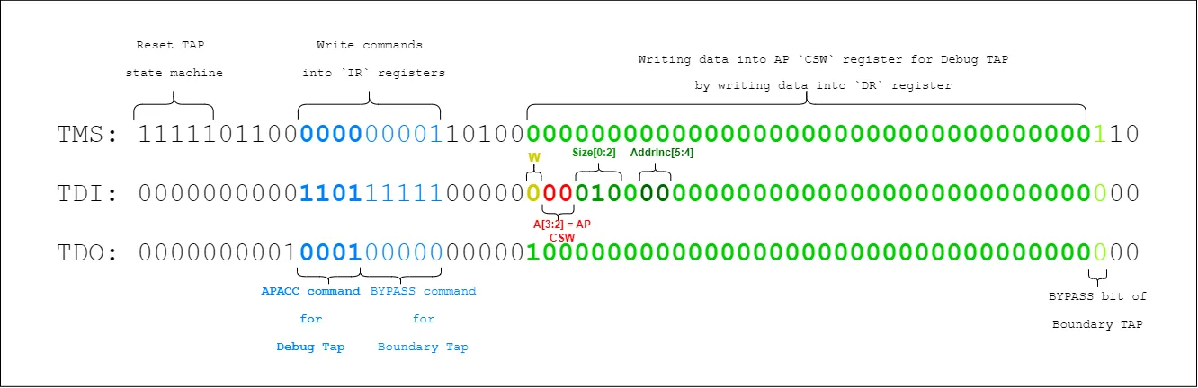
Next, we need to write the CSW register. Since this is an AP register, we need to use the APACC register to access it:
- Write
0b1011(theAPACCregister code) into theIRregister.
Create the data for the configuration: set the data size for writing to 32 bits (Size[0:2] = 0b010), disable the auto-increment function of the address (AddrInc[5:4] = 0b00). Write to DR.
- DATA[31:0] =
0x00000002 - A[3:2] =
0b00(address of CSW register) - RnW =
0b0

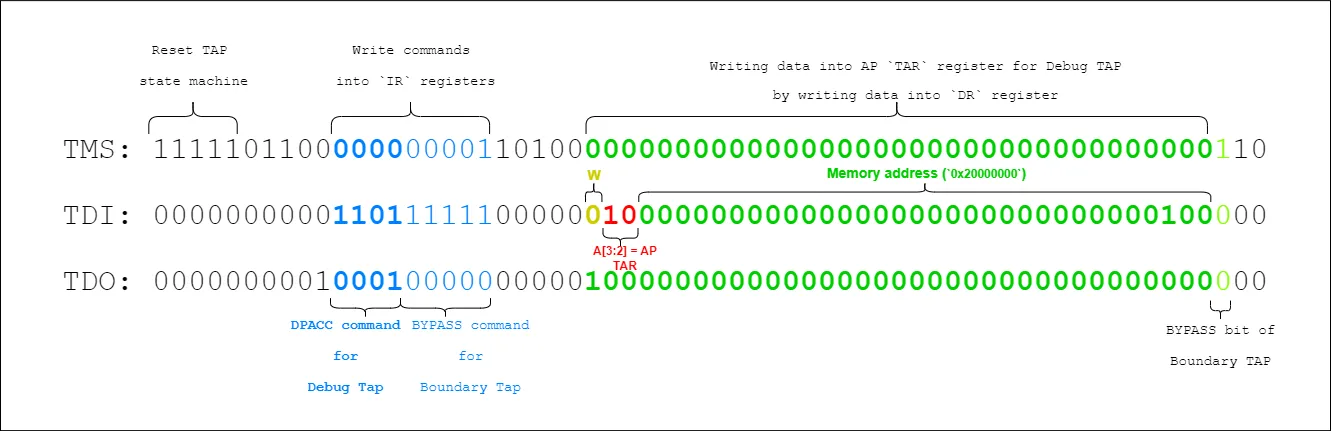
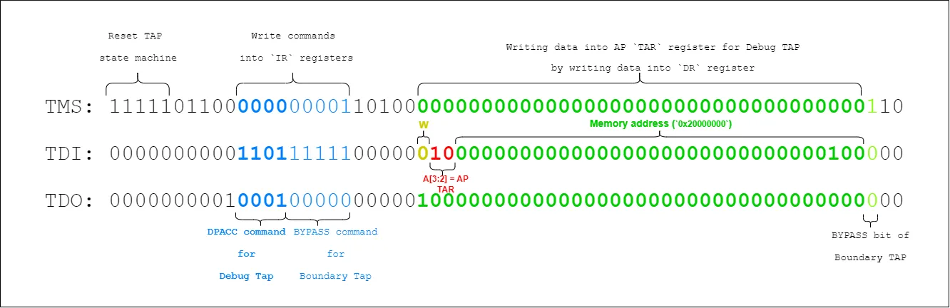
Then we need to set the address of the memory cell to which we want to write the data. This is done through the AP register TAR. And since this register belongs to the same AP as CSW and is in the same bank, we can omit the reference to the DP SELECT register and immediately write the address value. Write to DR:
- DATA[31:0] =
0x20000000 - A[3:2] =
0b01(address ofTARregister) - RnW =
0b0
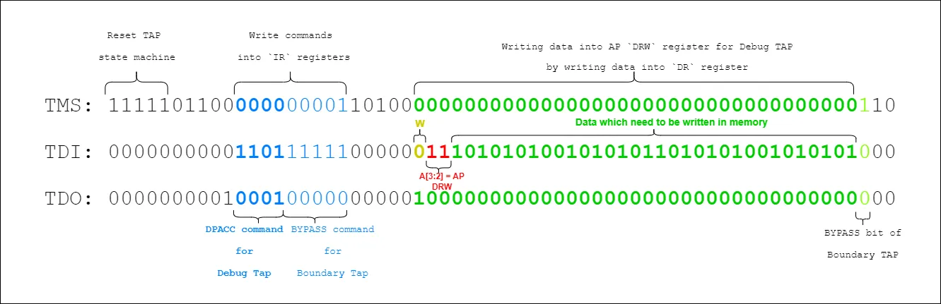
The last step is to actually write the data. To do this, we need to write them to the DRW register. Write to DR:
- DATA[31:0] =
0xAA55AA55 - A[3:2] =
0b11(address ofDRWregister) - RnW =
0b0
Reading a variable from memory
Let’s try to read the value from the memory cell at the address 0x20000000.
First, write 0b1010 (the DPACC register code) into the IR register. Next, we need to configure some settings in the CSW register of the AP. To access this register, we need to select the corresponding AP and register bank in the DP SELECT register. Using the data from the table, we form 35 bits of data that we write to the DR register:
- DATA[31:0] =
0x00 - APSEL[31:24] =
0x00 - APBANKSEL[7:4] =
0x00 - A[3:2] =
0b10(address ofSELECTregister) - RnW =
0b0
Next, we need to write directly to the CSW register. Since this is an AP register, we need to use the APACC register to access it:
- Write
0b1011(theAPACCregister code) into theIRregister.
We create the data for configuration: we set the data size for writing to 32 bits (Size[0:2] = 0b010) and disable the auto-increment address function (AddrInc[5:4] = 0b00). Write to DR:
- DATA[31:0] =
0x00000002 - A[3:2] = 0b00 (address of
CSWregister) - RnW =
0b0
Next, we need to set the address of the memory cell from which we will read the data. This is done through the TAR register of the AP. And since this register belongs to the same AP as CSW and is in the same bank, we can skip the DP SELECT register access and immediately write the address value:
- DATA[31:0] =
0x20000000 - A[3:2] =
0b01(address ofTARregister) - RnW =
0b0
We form a read request. To do this, we write to the DRW register:
- DATA[31:0] =
0x00 - A[3:2] =
0b11(address ofDRWregister) - RnW =
0b1
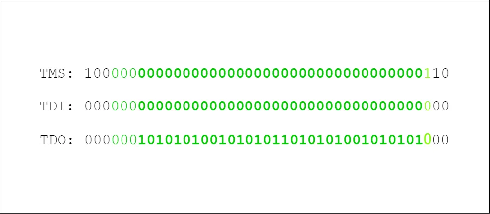
Read the DRW register by reading 35 bits from the DR register.
Interacting with the Processor Core
Well, we’ve explored how the debugger interacts with the microcontroller’s memory. Now, let’s delve into how the debugger can halt program execution, step through code, read the processor’s registers, and so on. In the case of the STM32F407VG microcontroller, this is achieved through special registers:
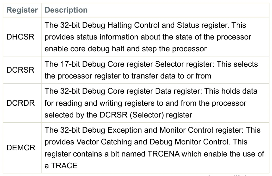
As detailed in section C1.6 Debug system registers of the ARMv7-M Architecture Reference Manual, these registers play a pivotal role in debugging.
What’s crucial for us now is understanding that by setting the C_DEBUGEN and C_HALT bits of the DHCSR register, we can halt the execution of the program. Similarly, by setting the C_DEBUGEN and C_STEP bits, we can execute the program step by step.
Access to these registers via the DAP module is essentially the same as accessing memory. Instead of providing a memory address, you provide the address of the desired register. For instance, in the case of the DHCSR register, the address is 0xE000EDF0. If you let me, I won’t delve into an example with the bit sequence since it would be identical to the example from the chapter on memory interaction.
Closing
Well, we’ve briefly explored how JTAG is used in microcontroller debugging. This topic is big, and it’s challenging to cover it fully within a single article. In this piece, we focused on invasive debugging, while non-invasive debugging wasn’t even mentioned. However, that wasn’t the goal when writing this article. For those who want to delve deeper into this topic, I recommend studying the links list listed below. As for us, we’ll move on, and in the next article, we’ll tackle the subject of testing printed circuit boards using the JTAG protocol.
Thank you for your time! :)
Note: This article was originally published by Aliaksandr on his blog. You can find the original article here.
See anything you'd like to change? Submit a pull request or open an issue on our GitHub
Links
- RM0090: Reference manual
- ARMv7-M Architecture Reference Manual
- Cortex-M4.Technical Reference Manual
- ARM CoreSight Architecture Specification
- DEBUGGING WITH JTAG
- Step-through debugging with no debugger on Cortex-M
- How do breakpoints even work?
- A Deep Dive into ARM Cortex-M Debug Interfaces
- Profiling Firmware on Cortex-M
 Aliaksandr Kavalchuk is a firmware engineer with over 10 years of experience.