Diving into JTAG - Overview (Part 1)
As the first segment of a three-part series on JTAG, this post will give an overview of JTAG to set up some more in-depth discussions on debugging and JTAG Boundary-Scan. We will dive into the intricacies of the interface, such as the Test Access Port (TAP), key registers, instructions, and JTAG’s finite state machine.
Table of Contents
Introduction
JTAG (Joint Test Action Group) is a specialized hardware interface based on the IEEE 1149.1 standard. This interface is designed to connect complex chips and devices to standard test and debugging hardware.
Nowadays JTAG is mainly used for:
- Output control of microcircuits
- Testing of printed circuit boards
- Flashing of microchips with memory
- Chip software debugging
The testing method implemented in the standard is called Boundary Scan. The name reflects the idea of the process: Functional blocks within the chip are isolated, and specific signal combinations are applied to their inputs. The state of each block’s output is then evaluated. The whole process is performed by special commands via the JTAG interface, and no physical intervention is required.
Test Access Point (TAP)
The Test Access Port (TAP) is one of the key elements of the JTAG protocol designed to control and configure chips connected to the JTAG chain.
The TAP operates as a simple finite-state machine that is controlled by the TMS (Test Mode Select) signal. It allows access to the internal registers of microcontrollers and other devices through JTAG commands.
Each device connected to the JTAG chain has its own TAP, which consists of the IR (Instruction Register) and DR (Data Register) registers. The IR the register is used to select the instruction to be executed on the device and the DR the register is used to transfer data.
Control signals
The Test Access Port comprises four mandatory signals (TCK, TMS, TDI, TDO) and one optional signal (TRST).
-
TDI(Test Data Input) — test data input. The commands and data are inserted into the chip through this pin on the rising edge of the signalTCK. -
TDO(Test Data Output) — serial data output. Commands and data are output from the chip through this pin on the falling edge of the signalTCK. -
TCK(Test Clock) — clock input. -
TMS(Test Mode Select) — controls the transitions between states of the finite state machine TAP. -
TRST(Test Reset) — reset signal of the TAP finite state machine.
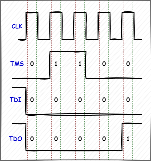
The standard is that the JTAG module reads data from the TMS and TDI lines on the rising edge of the TCK line. The JTAG module in any chip must also change the logic value on the TDO line on the falling edge of TCK. In the diagram below, the moments of reading data by the JTAG module are shown with the red dotted line and the moments of writing data are shown with the green dotted line.
Registers
The TAP state machine allows access to two special registers, the IR, and a symbolic register called DR.
The instruction registers store the current instruction to be executed. The value of this register is used by the TAP controller to decide what to do with incoming signals. The most commonly used instruction specifies which data register the incoming data should go into.
The Data Register is a placeholder for the register that is currently selected with the current content of the IR. Thus, IR is an index into a number of registers, and DR is the currently selected register. There are three main types of data registers:
- BSR (Boundary Scan Register) — The main register for testing. It is used to transfer data to and from the pins of the chip.
-
BYPASSis a single-bit register that transfers data fromTDItoTDO. It allows testing other chips connected in series with minimum delays. -
IDCODES — stores the ID code and revision number of the chip.
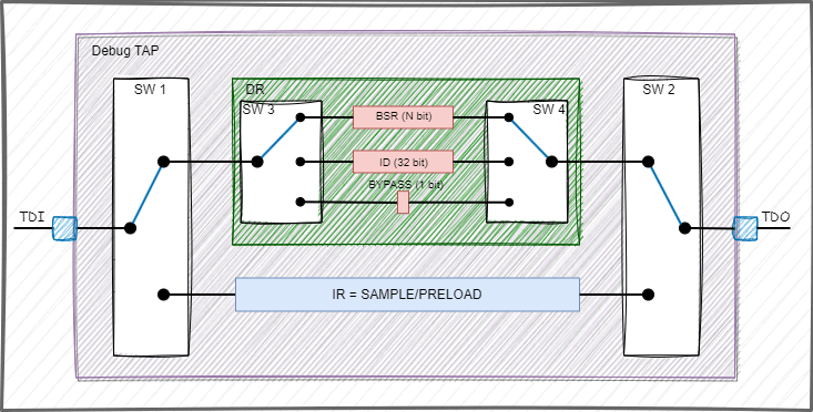
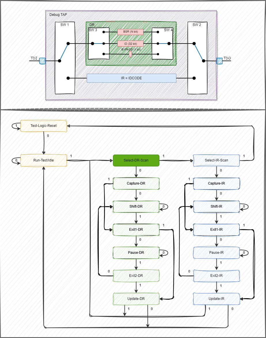
In the picture above you can see an approximate illustration of the principle of operation of the DR register: the switchers SW3 and SW4 choose the current register depending on the instruction in IR.
The size of the IR is implementation specific and usually varies between 4 and 32 bits. Since the selected register is directly accessed when scanning DR, the size DR depends on the current instruction.
JTAG registers are an important part of the microcontroller debugging process because they allow you to control and monitor the state of the microcontroller during program execution. Each microcontroller manufacturer may use its own JTAG registers, so you should consult the documentation of your particular microcontroller for details on the JTAG registers it supports.
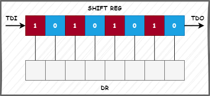
Shift register
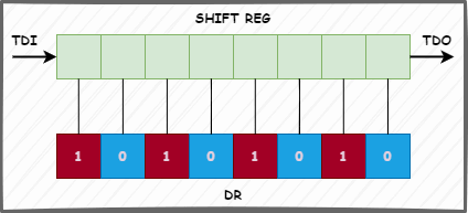
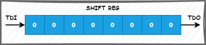
Data transfer (read/write) in the JTAG protocol is performed by the shift register principle. In a shift register, the data is transferred sequentially, bit by bit, one per clock cycle.
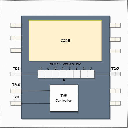
This register is located between the TDI and TDO pins and is used to receive information from the TDI pin and output information to the TDO pin. Every time you want to write something to the TAP via JTAG protocol - you set the necessary signals to the TDI pin - these signals are synchronously written to the shift register starting from the highest bit and gradually moving to the lowest bit of the register with each new clock, and the value of the lowest bit of the shift register with each clock is moved to the TDO pin, from which we can read it.
Note: I have not found detailed information about this anywhere, but from a general understanding, I can assume that for each register accessible via JTAG protocol, there is a separate version of the shift register. I.e. assuming we have we have a TAP with
IRregister 4 bits length,BYPASSregister 1 bit length,IDCODEregister 32 bits length, then for each of these registers there will be a separate version of the shift register which will be integrated into the scan chain betweenTDIandTDOpins every time the correspondingIR,BYPASS, orIDCODEregisters are selected. But this is just my assumption, which has not been documented yet.
JTAG Instruction
JTAG instructions are commands that interact with the TAP, enabling test, debug, programming, and configuration functions.
As described in the previous chapter even though selecting an instruction will usually not directly trigger any action, merely select the proper register as DR.
Let’s look at some of the most common instructions.
The IDCODE instruction
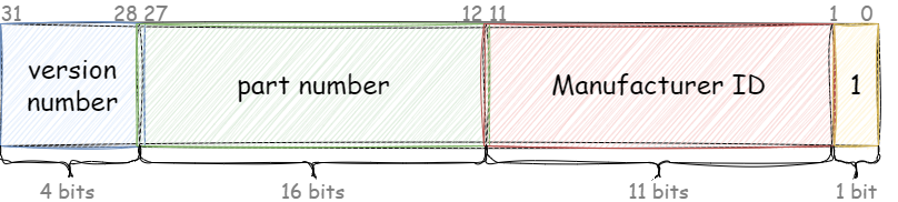
The IDCODE instruction in JTAG is used to get the unique identifier of the device connected to the JTAG circuit. Each device that supports JTAG has its own unique ID code, which can be read using the IDCODE command. This can be useful to identify the device type, manufacturer, and version.
This identifier is 32-bit in size and consists of next fields:
So when you load IDCODE instruction in IR register this will force the IDCODE register to be selected as the data register.
The BYPASS instruction
The BYPASS instruction in the JTAG protocol allows you to bypass one or more components in the JTAG chain without including them in the scan chain. This can be useful when the device does not support JTAG protocol commands or when you want to check other components in the chain.
When the BYPASS instruction is passed to a JTAG chain, it skips the device it is targeting and passes control to the next device in the chain. Thus, the BYPASS command avoids addressing a device that cannot be scanned by the JTAG protocol and continues to scan devices that are further up the chain.
In addition, the BYPASS instruction can be used to speed up a JTAG chain scan since skipping the device reduces the number of cycles required to go through the chain.
So when you load BYPASS instruction in IR register this will force the 1 bit BYPASS register to be selected as the data register.
The SAMPLE/PRELOAD instruction
Note: This command and a few others:
EXTEST,INTEST,HIGHZare actively used in the board testing process and will be discussed in detail in the second part of this article on the subject of using the JTAG protocol for board testing. In the same article they are specified by reference.
This command closes the TDI and TDO to the BSR (Boundary Scan Register). However, the chip remains in a state of normal operation. During the execution of this command register BSR can be used to capture data, which the chip is exchanged during normal operation. In other words with this command, we can read signals from the pin of the microcontroller without disturbing its operation.
So when you load SAMPLE/PRELOAD instruction in IR register this will force the BSR register to be selected as the data register.
State Machine
The JTAG protocol’s finite state automaton comprises a set of states that the TAP can assume, depending on the signals received at its inputs. Each state corresponds to a specific combination of signal values for the TMS and TDI inputs.
The transitions between states depend on the TMS signal at the moment of rising level of TCK.
The initial state after resetting is Test Logic-Reset. As defined by the standard the LSB is pushed in and pulled out first for all shift registers.
The State Machine is quite simple and has two ways of working:
- Instruction register selection (blue blocks) is used to select the current command.
- Data register selection (green blocks) is used to read/write data into the data registers.
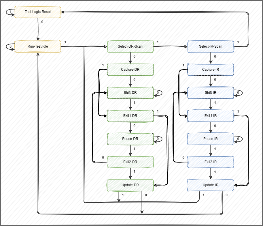
All states have two outputs, and transitions are arranged so that any state can be reached by controlling the dispenser with a single TMS signal (synchronized by TCK). There are two distinct sequences of states: one for reading or writing to the data register and one for working with the instruction register.
Let’s describe the most important states. But since IR path and DR path have identical states, I will describe these states for both paths at once specifying the differences if necessary.
- Test-Logic-Reset — all test logic is disabled, chip behaves normally.
- Run-Test/Idle — first state to initialize test logic and default idling state
-
Select-DR/IR-Scan — this state is necessary to select the current path: data or instruction. I think this can be visualized as the operation of the switches: SW1, SW1, SW3, SW4. When the Select-DR-Scan the state is hit, the switches SW1, SW1, SW3, SW4 are switched to the corresponding DR register. When the Select-IR-Scan state is reached - switches SW1, SW1 are switched to the
IRregister.
- Capture-DR — In this state, there is a parallel loading of the value stored in the selected DR register into the shift register if you follow the Select-DR-Scan state branch and loading of a special pattern if we follow the Select-IR-Scan state path, the value 0x01 is usually selected as the pattern.
-
Shift-DR — register shifts data from
TDIone step forwardTDO. The Shift-DR and Shift-IR states are the main states for serial-loading data into either data registers or the instruction register.
- Update-DR — the state in which the data in the shift register is written to the corresponding register in the chip. The Update-DR and Update-IR states latch the data into the registers, setting the data in the instruction register as the current instruction
-
Pause-DR/IR — temporarily halt data shifting from
TDItoTDO
The state machine progresses on the test clock (TCK) edge, with the value of the test mode select (TMS) pin controlling the behavior.
Note: Regardless of the initial state of the TAP controller, the Test-Logic-Reset state can always be entered by holding the TMS logic 1 for 5 clock cycles of TCK.
Example
Now that we’ve covered the theory, it’s time to see the JTAG protocol in action. Let’s consider an example where we read the ID code value from a chip, with an IR length of 4 bits.The sequence of bits on pins TMS, TDI, TDO, state machine transitions, and states of switches SW1 - SW4 are shown in the following gif:
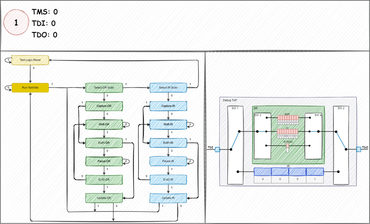
So, initially we are in the Run-Test/Idle state. In order to read the chip ID code we need to write the instruction code IDCODE into IR (let it be 0b1110 for our example). To write the instruction to IR we need to select the blue branch of our state machine. Images 2 and 3 show this transition. Image 3 shows how the keys SW1 and SW2 are switched when entering the Select-IR-Scan state. Next, at step 4 in the Capture-IR state, the 0b0001 pattern is loaded into the shift register. In step 5, a transition to the Shift-IR state is made and at this transition, bit 1 of the loaded pattern is advanced to the TDO pin.
Steps 6-7 show the sequential shift of the IDCODE (0b1110) instruction bit by bit into the shift register with the last bit being shifted in at the moment of transition to the Exit1-IR state (step 8). At step 9 (state Update-IR), the instruction code written to the shift register is latched into the IR register. At 10 we return to the initial state. We have written the instruction code, now we need to read the data corresponding to this instruction, for this purpose we will use the green branch of the automaton. At step 11 we go to the Select-DR-Scan state, at that the keys SW1 and SW2 are switched to the DR register and the ID register is selected because during the IR phase we selected the instruction IDCODE. In step 12 the Capture-DR state, 32 bits of ID code are loaded into the shift register. At step 13 the transition to the Shift-DR state is performed and at this transition the low-order bit of the ID code is advanced to the TDO output. Steps 14-20 show the sequential shift of the chip id code (0b111001101) bit by bit. At step 21, a transition to the Exit1-DR state is made and the last bit of the ID of the code is promoted. Step 22 (Update-DR state) - there should be a latch of the code written to the shift register into the selected DR register, but in case of IDCODE command this does not happen. At step 23 we return to the initial state again.
In Part 2 of this series, we’ll dive into debugging with JTAG.
Note: This article was originally published by Aliaksandr on his blog. You can find the original article here.
References
- Introduction to JTAG and the Test Access Port (TAP)
- The JTAG Test Access Port (TAP) State Machine
- JTAG.FPGA4Fun
- EEVblog — What is JTAG and Boundary Scan?
- Bringing JTAG Boundary Scan into 2021
- JTAG Implementation in Arm Core Devices
- Jworker — How it works
- DEBUGGING WITH JTAG
- The Intel JTAG Primitive — Using JTAG without Virtual JTAG
- Programming a Spartan-6 FPGA via JTAG
- Boundary Scan/JTAG
- Blackbox JTAG Reverse Engineering
- Blackbox JTAG Reverse Engineering — video
- Ghetto Tools for Embedded Analysis — Nathan Fain — REcon 2011
 Aliaksandr Kavalchuk is a firmware engineer with over 10 years of experience.