Diving into JTAG — Boundary Scan (Part 3)
In the third installment of this JTAG deep dive series, we will talk in-depth about JTAG Boundary-Scan, a method used to test interconnects on PCBs and internal IC sub-blocks. It is defined in the IEEE 1149.1 standard. I recommend reading Part 1 & Part 2 of the series to get a good background on debugging with JTAG before jumping into this one!
Table of Contents
The Principle of Boundary-Scan
The principle of operation is that special cells — scan cells — are inserted between the physical pins of the chip and its internal logic.
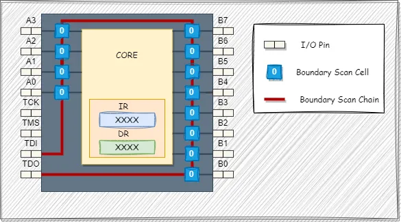
In normal mode, these cells are transparent and the core is connected to I/O ports. In boundary scan mode, the core is isolated from the ports, and the port signals are controlled by the JTAG interface.
The boundary scan cells are connected to a serial shift register, which is
referred to as the boundary scan register (BSR). This register can be used to
read and write port states.
In general, the principle of Boundary-Scan operation is that with the help of special JTAG commands, it is possible to set values in the scan cells and, through them, influence the chip pins.
Following boundary scan instructions are defined in the IEEE standard:
-
BYPASS(mandatory):TDIis connected toTDOvia a single-shift register. -
SAMPLE(mandatory): Takes a snapshot of the pins of the IC. -
PRELOAD(mandatory): Loads data to the boundary scan register. -
EXTEST(mandatory): Apply preloaded data of the boundary scan register to the ports. -
INTEST(optional): Apply preloaded data of the boundary scan register to the core logic. -
CLAMP(optional): Apply preloaded data of the boundary scan register to the ports and select theBYPASSregister as the serial path betweenTDIandTDO. -
HIGHZ(optional): Places the IC in an inactive drive state (e.g. all ports are set to a high impedance state) and leavesBYPASSregister as the selected register.
The structure of the boundary scan chain and the instruction set are described with the Boundary Scan Description Language (BSDL). BSDL is a subset of the Very High-level Design Language (VHDL). The BSDL files are provided by the IC manufacturer. The BSDL language will be covered in the next article, so we will not describe it in detail here.
The Boundary Scan Cells
As mentioned above, scan cells are the core element that makes Boundary Scan possible. These cells can be programmatically configured to perform various functions, such as transmitting or receiving data, allowing you to test connections between chips without having to physically access the pins.
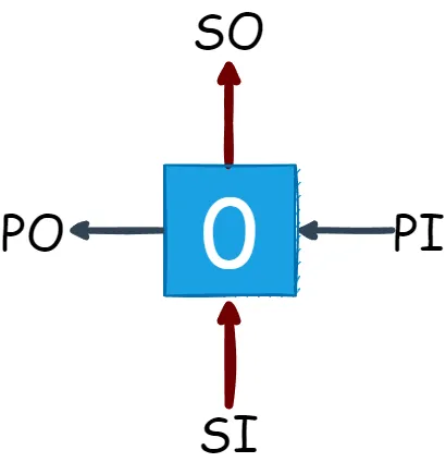
Each boundary-scan cell can:
- Capture data on its parallel input
PI - Update data onto its parallel output
PO - Serially scan data from
SOto its neighbor’sSI - Behave transparently:
PIpasses toPO
At the device level, the boundary-scan elements contribute nothing to the functionality of the internal logic. The boundary-scan path is independent of the function of the device.
The boundary-scan cells must be provided on all device digital input and digital output signal pins, except Power and Ground.
Scan cells can be categorized by functionality into the following types:
-
Input Cells: Used to monitor input signals.
-
Output Cells: Used to control the output signals:
-
Output2: This cell type does not support three-state logic. It can set the pin to state “0” or “1”. -
Output3: This cell type supports three-state logic, allowing a pin to be in the “0”, “1” or “Hi-Z” (high impedance) state.
-
-
Bidirectional Cells: Can be used for both input and output. Cells of this type typically support three-state logic.
-
Control Cells: Used to control other cell types:
-
Control: This cell type can control the functionality of one or more other cells, for example, by switching them between input and output modes. This cell is not connected to the chip pins -
ControlR: This cell type is similar to theControltype but with the additional ability to read the state of the controlled cells. This cell is not connected to the chip pins.
-
-
*Clock Cell: This function indicates that this cell is connected to the system clock frequency, which allows
INTESTmode operation.
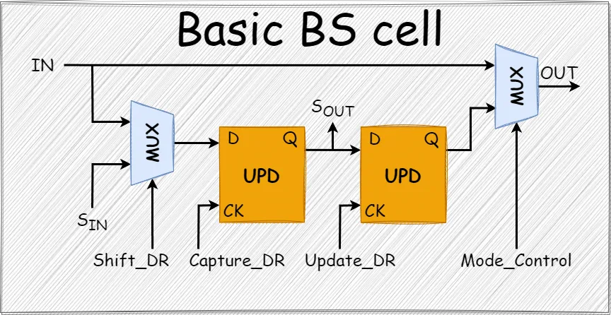
Each scan cell typically consists of a small set of flip-flops and logic elements that allow it to perform various functions such as storing data, transferring data to other cells, etc.
In general, a scan cell can be represented by the following scheme:
A Boundary Scan cell’s internal architecture can be highly different. In its
version from 2001, the IEEE Std. 1149.1 describes ten different cell types
(BC_1 to BC_10):
-
BC_1– The basic Boundary Scan cell that can be used as input, output, control, and internal cells. Supports all instructions. -
BC_2– Boundary Scan cell that can be used as an input cell. Cell architecture is likeBC_1except a multiplexer in the signal patch at the entrance to the cell from the Parallel input. -
BC_3– Cell only used for inputs or internal cells as it does not possess an Update latch, but it does support theINTESTinstruction. -
BC_4– Like theBC_3, this cell does not possess an Update latch. Also, a multiplexer has been removed from the system signal path. Removing the multiplexer removes some potential signal delay through the cell. This cell cannot be used on any input pin except a system clock. -
BC_5– Cell can be used as a merged cell application. Merged cells act as an input cell, thus satisfying the requirement that an input pin have a cell and it can also serve to drive the enable of an output driver. -
BC_7– Cell can provide data to the output driver and also monitor pin activity even when the output drive is driving the pin. -
BC_8– Cell monitors only the pin driver output and therefore does not support theINTESTinstruction. -
BC_9– A self-monitoring cell for outputs that support theINTESTinstruction. -
BC_10– A self-monitoring cell that does not support theINTESTinstruction.
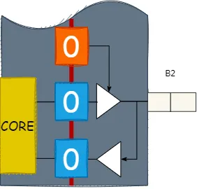
The number of cells need not necessarily match the number of chip pins. For
example, if the chip pin is bidirectional (pin B2 in Figure 4), conceptually
at least, three boundary-scan cells are required: one on the input side, one on
the output side, and one to allow control of the IO status. In practice, the two
IO scan cells are usually combined into a single multi-function cell called a
BC_7.
The Boundary Scan Register (BSR)
Boundary Scan Register (BSR) is one of the data registers (DR) consisting of
a sequence of scan cells (Boundary-Scan Cells). Figure 5 shows how the scan
cells are linked together to form the boundary-scan register. The order of
linking within the device is determined by the physical adjacency of the pins
and/or by other layout constraints. The boundary-scan register is selected by
the EXTEST, SAMPLE, PRELOAD, and INTEST instructions.
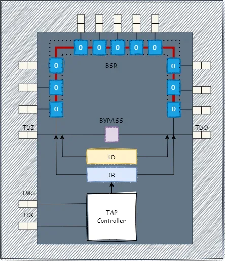
During scan operations, data is shifted BSR in the direction from TDI to
TDO. The values in the scan cells can be changed or read, allowing testing to
be performed.
The size and format of this register determine the number and sequence of scan
cells in a particular chip - i.e., before testing, it is necessary to find out
the length and format of the BSR register. This information is supplied by the
manufacturer in the BSDL file format for a particular chip. Here is an example
of a truncated BSDL file for the STM32F407 microcontroller:
num       cell        port     function
405       BC_1,        *,      CONTROL,
404       BC_1,        PE2,    OUTPUT3,
403       BC_4,        PE2,    INPUT,
where,
-
num: Is the cell number. -
cell: Is the cell type as defined by the standard. -
port: Is the design port name. Control cells do not have a port name. -
function: Is the function of the cell as defined by the standard. Is one ofinput,output2,output3,bidir,control, orcontrolr.
We can see from this file that:
- The number of scan cells, and consequently the length of the
BSRregister is 405 pieces/bit. - One I/O pin can have 3 scan cells which are divided according to the
functionality to be performed:
CONTROL,OUTPUT3,INPUT.
This information must be considered when forming the contents of the register
BSR.
The Boundary Scan Instructions
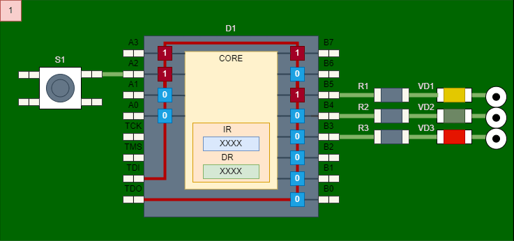
SAMPLE Instruction
This command reads the current values from the scan cells and passes them to the
TDO output. This is useful for reading the current state of the chip pins.
This command causes TDI and TDO to be shorted to the BSR register.
However, the chip remains in the normal operating state. During the execution of
this command, the BSR register can be used to capture the data exchanged by
the chip during normal operation. In other words, with this instruction, we can
read signals from the microcontroller output without disturbing its operation.
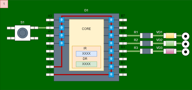
In step 3, when the SAMPLE instruction is loaded into the IR register, the
signal is read from the pins to the scan cell. In the next steps, we move to the
Shift-DR state and read the BSR register along with the value of the pins
received in the previous step. Note that when the read unit passes through the
scan cells bound to pins B3, B4, B5 the LEDs connected to these pins do
not light up, because at the moment the scan cells are not connected to the chip
pins.
PRELOAD Instruction
This command allows you to preload certain values into Boundary-Scan Cells for later testing or other operations.
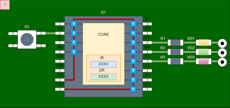
Here, everything is simple. After writing the command PRELOAD, we just need to
write the values in the scan cells to the register BSR for the corresponding
pins in the state Shift-DR. And again, note that after writing all the values
to the scan cells, the LEDs connected to pins B3, B4, B5 do not light up
either.
SAMPLE/PRELOAD Instruction
Sometimes two commands: SAMPLE and PRELOAD are combined into one. When
writing this command to the IR register, the values of the pins are read into
the scan cells (BSR register) and then in the Shift-DR state we read these
values and write new values for the pins into the scan cells (BSR register).
Again, after the SAMPLE/PRELOAD instruction is completed, has no effect on the
pins themselves.

Typically, the SAMPLE/PRELOAD command is the first command to be executed
during Boundary Scan testing, and it serves as the basis for many other
operations.
EXTEST Instructions
The EXTEST command in JTAG is used to test external circuits connected to the
microcontroller pins. When the microcontroller is in EXTEST mode, all its
function blocks are disabled and the microcontroller pins can be used to test
the connected external circuits for short circuits, open circuits, etc. This
command can be used to verify the pins and circuits of a microcontroller during
the manufacturing process and to verify that external circuits are properly
wired during development.
This command is the one for which we wrote values to the scan cells in the
PRELOAD command. Because exactly EXTEST makes the scan cells transfer the
values of the signals stored in them to the output.
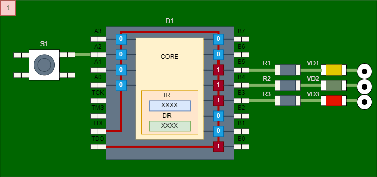
After using this command, the I/O pins are disconnected from the internal logic of the microcontroller and you can no longer control them from the program.
INTEST Instructions
It is also possible to use boundary-scan cells to test the internal functionality of a device. This use of the boundary-scan register is called Internal Test, shortened to Intest. Intest is only really used for very limited testing of the internal functionality to identify defects such as the wrong variant of a device or to detect some gross internal defect.
Test Example
Let’s see how to use the SAMPLE/PRELOAD and EXTEST instructions to test the
board for a fault.
Let’s imagine that we have the following situation: two chips D1 and D2
connected to each other through pins 5,6,7 for chip D1 and 2,3,4 for chip D2
and we need to check that these connections work correctly. But let us assume
that a solder bridge has formed between pins D1:6,7 and D2:2,3. The
described situation is presented in the figure 11.
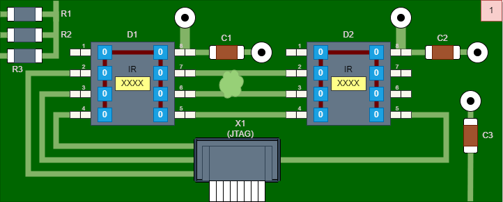
So what can be done using JTAG to check the connection of chips D1 and D2:
- Load into chip
D1using thePRELOADcommand the template:0b0101010000. - Use the
EXTESTcommand to output the generated test pattern to the chip pins. - Using the
SAMPLEcommand for theD2chip, we read the pin states and expect the following result:0b00001010, but we get0b00001000, i.e., there is an incorrect signal on pin 2 of chipD2, so the connectionD1:7<–>D2:2has some problems.
Conclusion
As Socrates said, “The more I know, the more I realize I know nothing.” Indeed, this is a challenging topic that has made me realize there is so much more complexity to JTAG than meets the eye! Any suggestions on things I may have overlooked are most welcome. Engage with me in the comments – I look forward to hearing from you!
Note: This article was originally published by Aliaksandr on his blog. You can find the original article here.
See anything you'd like to change? Submit a pull request or open an issue on our GitHub
Links
- Boundary-Scan Tutorial
- JTAG Instruction Registers | Boundary Scan Cell | Sample | Preload | Extest | Intest | HIGHZ |
- JTAG Test
- Testing Digital Systems I. Lecture 5: Fault Models
- Everything You Need to Know About ScanWorks Interconnect Part 6: Boundary Scan Cell Descriptions
- JTAGULATOR
- jtag-boundary-scan
- Boundary Scan Basic Tutorial
- OpenOCD boundary scan on STM32
- Lauterbach: Boundary Scan User’s Guide
- 12 3 DFT2 JTAG Instruction
- 12 4 DFT2 Instruction2Conclude
 Aliaksandr Kavalchuk is a firmware engineer with over 10 years of experience.