Smart Ring Development (Part 2) - Hardware Design
This series of articles discusses the development of a SOTA Open Smart Ring - a tiny wearable packed with electronics that fits on your (even the smallest) finger. We dive deep into what it means to develop such a product, its challenges, and ultimately, how to make it a manufacturable and usable piece.
In the first part of this series, we looked at a higher level at what is inside a smart ring. We’ve also researched some of the available smart rings on the market and looked at prototyping one. In this article, we’ll dive deeper into the hardware of Open Ring - an open-source smart ring project. By the end of this article we’ll have looked at all the aspects of the hardware design and you will learn all the tricks we used to bring this project to life!
PCB stackup
If we want to keep the smart ring as thin as possible (e.g., Oura Gen 4 is at 2.9mm), our PCB needs to be as thin as possible. The PCB will have to bend and follow a ring shape, so we’re definitely looking at a flexible PCB. However, not every component can be soldered onto a flexible PCB, and survive the stresses caused by bending (think of all the BGAs), so it’s sensible to have a rigid board as well.
That leaves us with a rigid-flex board, where parts of the PCB are flex and others are rigid. The flex PCB stackup serves as the base, and the rigid part is done by just sandwiching some more PCB layers on top of the flex. Flex PCBs can be made very thin, which is a great advantage, and they generally support full vias only. In the rigid part, these vias basically serve us as “free” buried vias. After adding the rigid part, we can also have full thru vias, and we can also get laser microvias (only from the outermost layer to the first next copper layer).
The total stackup that would satisfy high-density component requirements is
shown below:
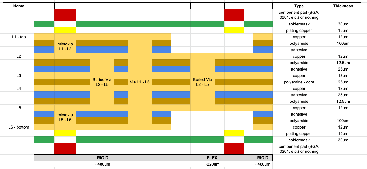
The flex part has 0.22mm, and the flex-rigid part sits at 0.48mm. Thinking of
the component budget, if the aim is 2.9mm thickness, and assuming we need a
minimum of 0.2mm silicon outer layer, that leaves us at
 of max component height on each side if the components bent along the ring
curve. Since they don’t bend, we’re working with some extremely tight spaces
here. Square chips in BGA and WLCP packages under 3mm width shouldn’t be a
problem, but some capacitors and inductors might get troublesome due to their
height, so we’ll be extra careful when selecting those. The general rule of
thumb is that we want to keep components as flat as possible, and put all tall
components in the middle of the rigid parts to compensate for the ring
curvature.
of max component height on each side if the components bent along the ring
curve. Since they don’t bend, we’re working with some extremely tight spaces
here. Square chips in BGA and WLCP packages under 3mm width shouldn’t be a
problem, but some capacitors and inductors might get troublesome due to their
height, so we’ll be extra careful when selecting those. The general rule of
thumb is that we want to keep components as flat as possible, and put all tall
components in the middle of the rigid parts to compensate for the ring
curvature.
BLE processor
The heart of the smart ring, and the centre of communication with the outside world, will be the BLE MCU you choose. Even with Low Energy in the BLE acronym, Bluetooth communication can still take up a significant part of your energy budget, depending on the application. Health tracking smart rings, such as Oura, can generally store measurements and sync them later, reducing this worry. However, if the solution needs to perform an action in real time (such as gestures on the ring controlling music on the phone), the BLE needs to be always ready to send requests through. Fortunately, many of the BLE SoCs have advanced sleep capabilities, allowing a solution to achieve this in a smart way with minimal power usage.
We’ve settled on Dialog’s DA14531. It was ahead of its time due to very low cost at high quantities, very clean SDK, and very high efficiency of BLE transmission. It didn’t come with all-advantages though. This chip has the old school one-time-programmable memory for bootloader (you can’t go wrong programming that), external FLASH requiring a separate chip on board, and it generally runs code from system RAM, which is limiting. Another great option that was considered was Nordic MCUs such as nRF52805 in a 2.5x2.5mm WLCSP package. Generally, it’s better to get more FLASH and RAM and not worry about the firmware upgrades (as well as security updates, which in the BLE world are common).
An important consideration around the BLE chip is the crystal. A typical BLE crystal will be 32MHz, and it will provide the base for the high-frequency radio signal. Care must be taken when selecting such a crystal, as due to aging, the frequency of the crystal can shift and render the product useless. Dialog’s recommendation around this is 10ppm base frequency tolerance and only 2ppm aging per year. Such crystals will often be marked as “BLE application”. You can find datasheets of crystals that adhere to this requirement here. Notably, the one we ultimately chose was Abracon’s ABM12W (low height and RoHS-compliant BLE crystal).
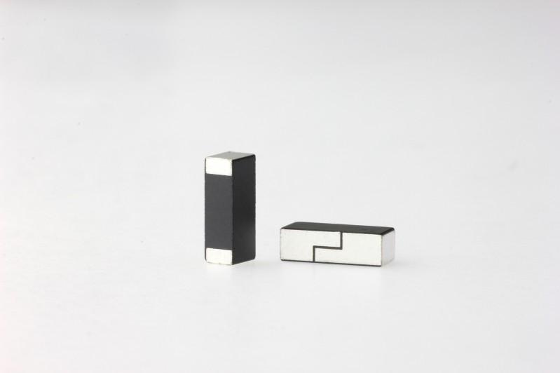
BLE antenna
Closely tied to the BLE processor is the BLE antenna. The antenna design is generally independent of the chip itself, since the carrier frequency is the same 2.4GHz. Often considered as “black magic”, the antenna design is indeed a solid piece of engineering. Oura had a job position of “Senior RF Antenna Design Engineer” just for this. After all, a product that emits radio waves falls under the FCC category, so to be able to commercialize it, it requires a range of certificates, including those for emitted radiation. A poor antenna design not only comes with low effectiveness but can also cause interference to other radio devices.
From the teardown of the Oura Ring Gen 3, we learned that their antenna was designed as a microstrip antenna directly on the PCB. This is probably the best way to go, and offers full flexibility, but is also the most expensive in terms of development effort.
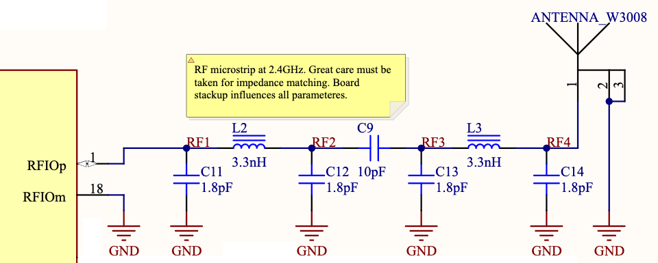
For these reasons, we opted for a simple integrated antenna component. It takes up space on the PCB and is a bit tall, but it offers a packaged solution. Still, a microstrip is required to route the 2.4GHz signal from the BLE chip to the antenna, and this part of the PCB needs utmost care! It is a good practice to share this information on a separate mechanical layer with the PCB manufacturer, so they can adjust the microstrip accordingly to the stackup directly in the gerber files.
Below is the microstrip part as seen on the schematic:
Power management
A smart ring needs a battery, and a battery requires charging and battery management circuitry. Thankfully, integrated solutions exist that take care of both. One of them is Texas Instruments’ BQ2512x series (e.g. BQ25125), an intelligent battery charger with integrated DC/DC. This IC offers a couple of really cool features:
- high efficiency (we do not want to waste power due to voltage conversion)
- safe battery charging with a temperature sensor
- shipping mode (equivalent to ultra-sleep mode to preserve the Li-Ion battery life during product shelf time)
- load switch controlled programmatically
The really cool feature that we want is the shipping mode, as we do not want the Li-Ion battery to deplete and lose its full capacity, which is irreversible. This battery depletion can happen not only during shipping or warehouse storage when the ring is waiting for its new owner, but also if the customer stops wearing the product for a while. If the battery depletes to very low levels (close to 3V), we want to always enter the shipping mode for battery protection. For this reason, our UX “0%” battery level needs to be mapped to a voltage slightly higher than 3V, which is when irreversible battery damage starts happening, to act as a safety margin.
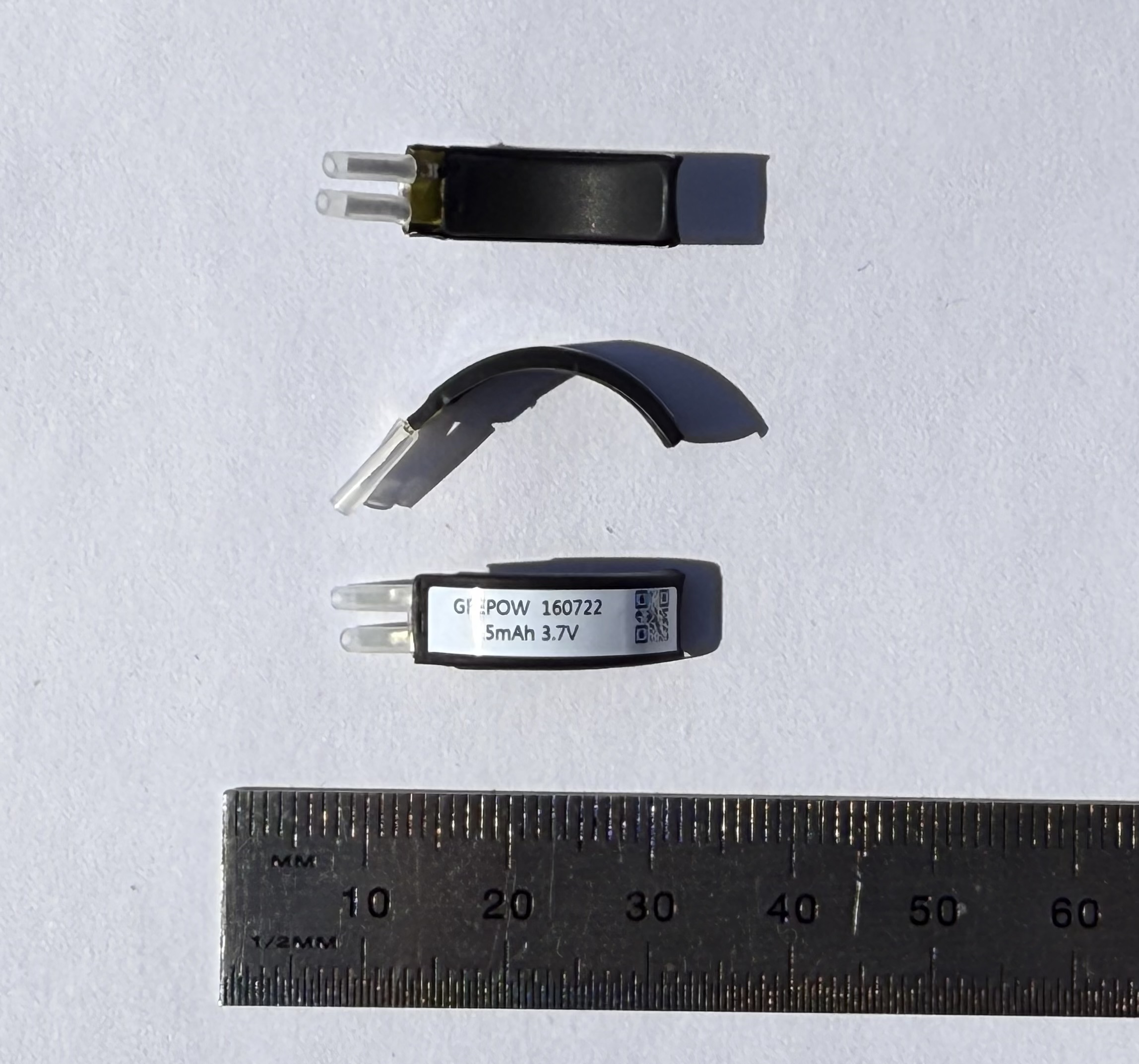
The power management circuit can be paired up with a
Grepow curved battery,
perfect for electronics that wrap around the finger:
BQ25125 will provide 1.8V for our system voltage, which will be used by all other ICs. Dialog’s BLE chip will additionally make its own 1.1V rail.
With power circuitry resolved, we’re still left with charging the battery.
Wireless charging
Basically, we can either charge the smart ring via physically exposed contacts or wirelessly. Physical contacts, while very simple on the electronics design level, come with their own mechanical challenge. Pads need to be exposed, they need to be invulnerable to a variety of environmental factors (sweat, water, ESD, etc.), they need to align perfectly with charger contacts, and maintain good pressure during charging.
All things considered, physical charging contacts are quite hard to get right with product longevity and good user experience in mind. The other option is wireless charging through induction. A wireless induction charger is a form of an air-gapped transformer. Sounds pretty easy, right?
The induction charger consists of a primary and secondary coil, an air gap, and housing material between them. The primary coil and secondary coils form simple LC circuits, tuned in frequency to one another. The primary coil needs only a simple square PWM drive to excite the LC circuit. It’s important to get the frequency of the charger right, since the charger will also need to pass FCC tests for emitted radiation. One of the most widely used frequencies for wireless power systems is 6.78 MHz (half of the popular 13.65 MHz for NFC/RFID). At 6.78 MHz, we can make a coil simply out of the PCB tracks with an added ceramic capacitor to form our LC circuit.
Our receiver coil on the smart ring side requires only a very simple half-bridge rectifier made of two Schottky diodes. It’s important to pick fast Schottky diodes with low parasitic capacitance, since we’re operating at 6.78 MHz here. The rectifier gets us from induced AC into sweet DC, which we can work with. We also add a few chunky capacitors to maintain a steady voltage, and a Zener diode in case we’re inducing higher voltage than our BQ25125 can take, and we’re done!
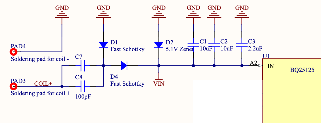
To get the induction charging right, the most important bit is getting impedance matched. The primary LC circuit in the ring charger needs to be tuned to the secondary LC circuit in the ring. This also needs to account for all mechanical offsets, like the tolerances of the coil placement in both the ring and the charger, and the tolerance of the ring sitting in the charger during charging (it will never sit perfectly).
With this in mind, we arrive at a big design decision. Do we make one charger to rule them all (account for all ring sizes)? Or do we make multiple chargers (one per ring sizing)?
Ring sizes
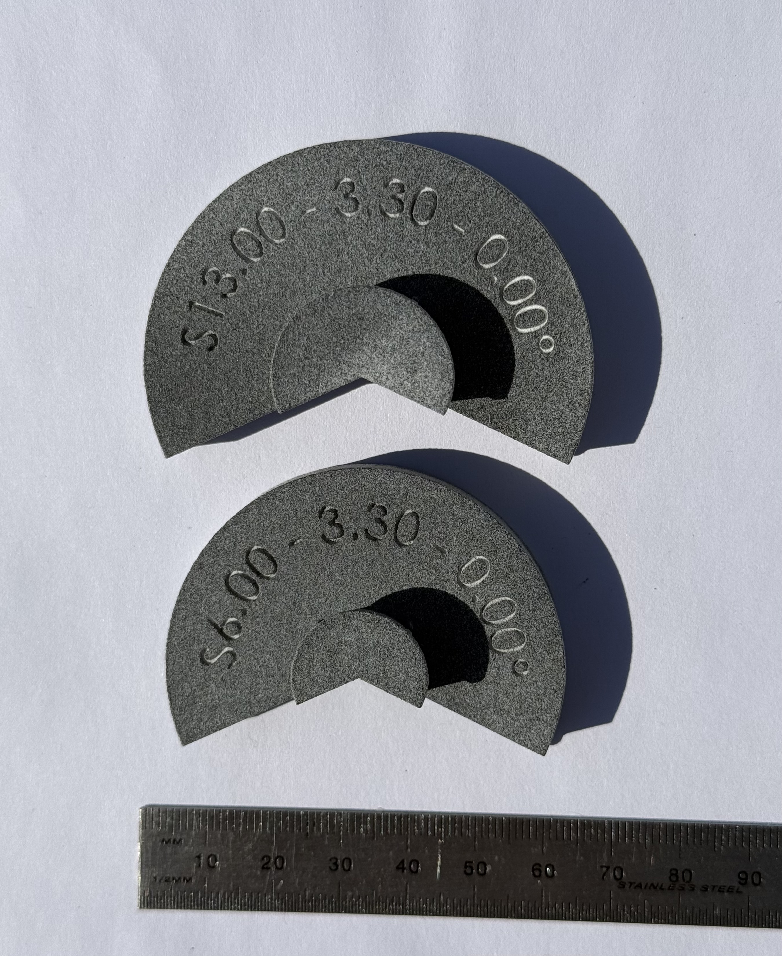
When it comes to user experience, it’s best to have a ring made per finger size. Most common ring sizes range from US6 to US13, which follows the general population’s ring finger distribution. This means to accommodate the most popular sizes, we need to make the product in 8 sizes (if that sounds like a pain, then yes, it is)!
Another option that is significantly easier to manufacture and manage is to group the sizes, often done in 3 discrete groups of S (small), M (medium), and L (large).
It’s a common practice (same as you can see with smartphones) to put a bigger battery in a larger ring, so with a greater ring size, the customer also gets longer battery life.
The design around ring sizes needs to be based on the balance between manufacturability and user experience. It will affect managing physical product stock, the whole mechanical design, battery life, automated test equipment, and other things.
The way Open Ring was designed was to accommodate multiple ring sizes. The PCB needs to be flat (component-free) at the part where the battery goes, so we reuse that part for the touch sensor on the other side. This part can be cut to different lengths as it exposes the copper pads to connect both the vibration motor and the charging coil. This was a cheap way for us to support different ring sizes; however, had the original product been a success, we would have made a PCB for each ring size and embedded the charging coil directly into the main ring PCB.
Touch and gestures
The main feature of Open Ring is the touch sensor, as it captures user input. The original idea was to use taps and swipes to control music (e.g., on a user’s smartphone), but these gestures can generally map to any allowed Bluetooth action.
There are a few ways to detect gestures like this, with the most popular one being capacitive sensing. Capacitive sensing detects changes in capacitance that are caused by the human body. There are two main techniques to measure capacitance for touch: self-capacitance and mutual capacitance. In very simplified terms, a self-capacitance measurement circuit will measure the capacitance of a touch pad (along with all the parasitic capacitance), while a mutual capacitance circuit will measure the difference in capacitance between two wires. A mutual capacitance circuit is more complicated, but yields better results, lower noise, and better resistance to environmental factors.
It’s worth mentioning here an interesting find in Oura Gen 3 X-ray teardown photos. The PCB hosts two large copper pads, which are most likely self-capacitance wear detection circuitry, especially due to Oura using a Cypress chip known for CapSense technology.
There are a few chip manufacturers that offer capacitive sense technology. This capability will either be provided as one of the MCU peripherals or in a standalone chip. With mutual capacitive sense, due to its more complex nature (and therefore, setting up and tuning), the reasonable approach was to pick an MCU.
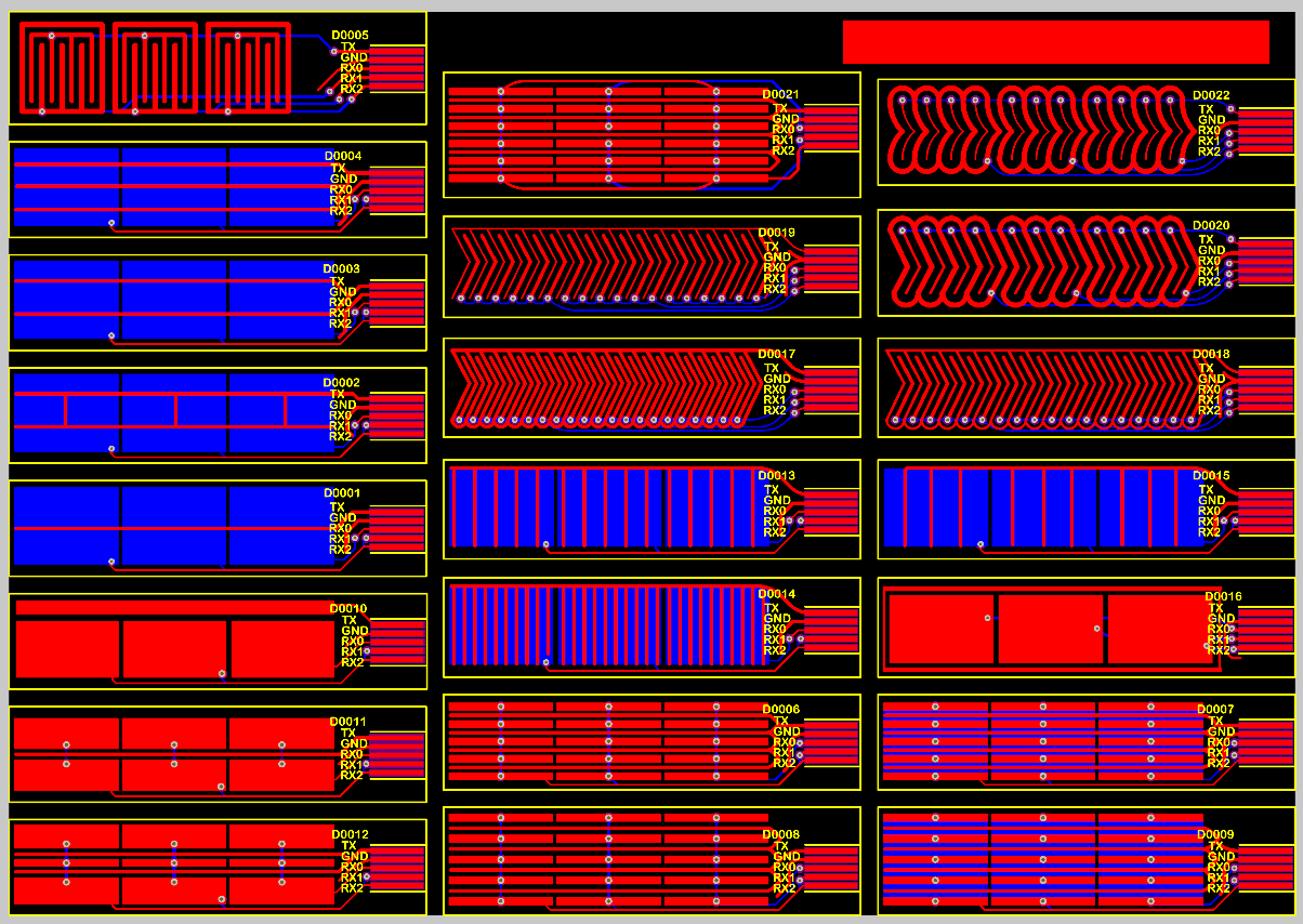
It’s worth noting that picking the chip is only the first step. The touch sensor
needs to be designed correctly using PCB copper layout. We’ve tried many
different mutual capacitance designs to pick the one that works best in a ring:
As for the MCU, we chose Atmel ATSAML10E16A with QTouch in a tiny 2.8x2.8mm WLCSP package (remember: everything needs to be absolutely tiny in a smart ring). This increases the complexity of the product a fair bit due to dual MCU architecture, rather than having a single all-in-one SoC. However, after a few prototypes with different chipsets at the time, we concluded this was the best chip for this application. The architecture has a Dialog BLE chip acting as the interface to the outside world, while Atmel handles the real-time part: gesture sensing, haptics, wear detection, and battery charging. The obvious challenge introduced by this architecture is complexity of the firmware update process, where both MCUs must update simultaneously, and they need to always be able to communicate with each other if for any reason one of them fails to update.
With capacitive sense design in place, we arrived at the last feature of the ring: haptics.
Haptics
Haptics is often paired up with some form of user input, in our case a touch sensor, to give the user feedback about performed action (it’s often called “haptic feedback” for this reason). If our sensor were replaced with physical buttons that one can push and feel (good luck fitting that in!), there would be no reason to put haptic feedback in the product.
However, with a touch sensor in a Bluetooth-connected device, things can go wrong fast! The user can touch the sensor by mistake, there could be a Bluetooth connection dropout, there could be water on the sensor, or mocking physical touch, just to name a few. These problems stem from the nature of touch sensing, as there is no immediate feedback for the user, hence why we introduced haptic feedback to the product.
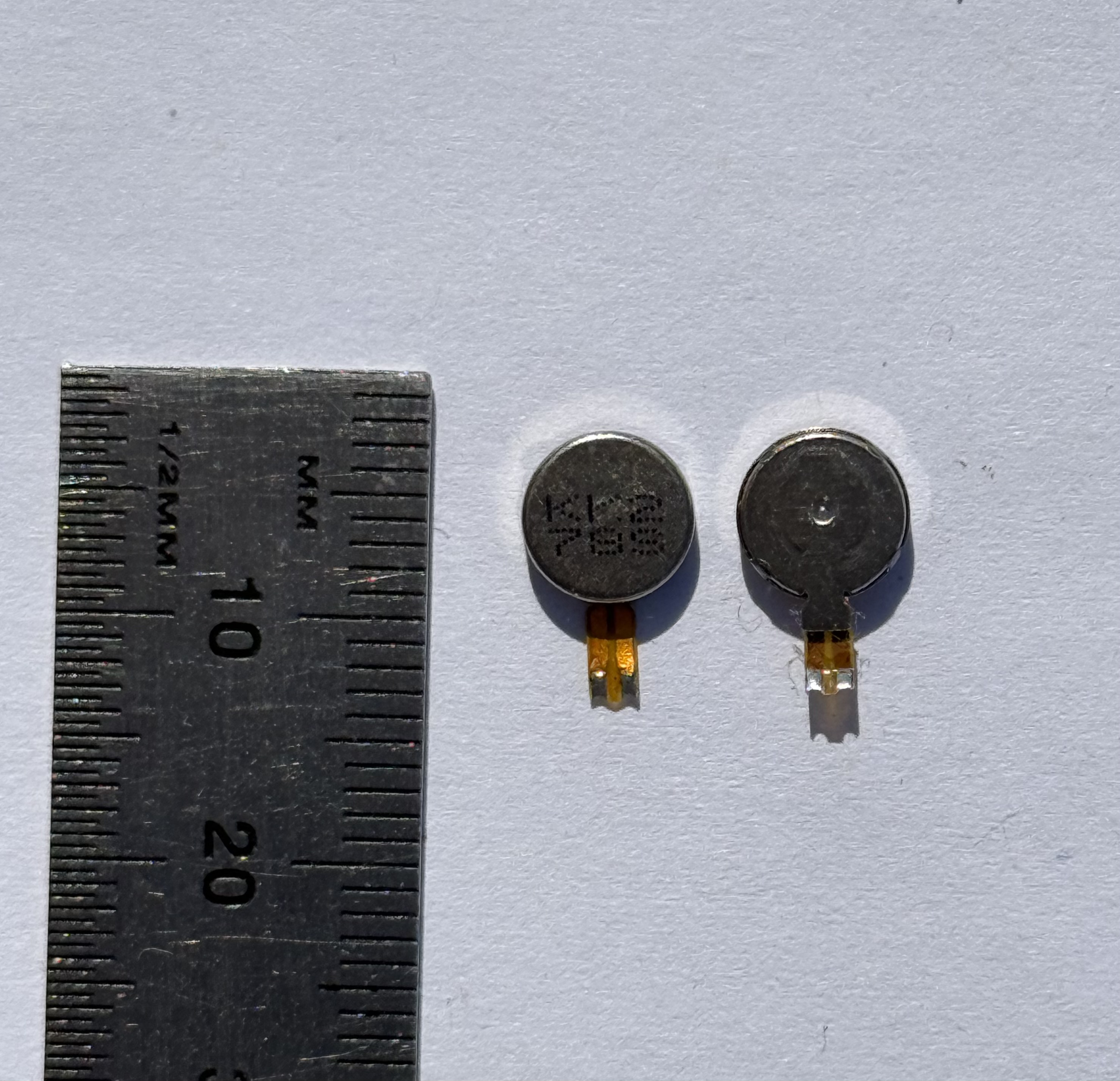
Haptic feedback is generally realised in the form of mass movement. This can be simply realised by having an off-centre mass in a motor. When the motor is actuated, the off-centre mass causes vibration. Another way can use piezoelectric material which deforms when electric field is applied, effectively causing a “click” feeling. This form of haptics has been used in Amazon’s discontinued Echo Loop ring.
These two options come with significant challenges when you’re trying to fit everything into a tiny smart ring. Piezoelectric actuators require a high voltage (over 50V) and a circuit for waveform generation. This circuit will usually consist of a boost converter (requires a coil) and an H-bridge. Integrated circuits exist like Texas Instrument DRV2667, but even this comes in a 4x4x1mm package, not counting all other necessary components, especially the piezo actuator.
On the other hand, vibration coin motors are extremely simple to drive. Like any other DC motor, all they require is a switch. The significant disadvantage, however, is the startup current, often in the 100mA+ range, which is needed to get the mass into initial motion. A small curved Li-Ion battery of 17mAh capacity cannot supply such a current. In the best case, we’re looking at a 3C rate at 17mAh, which results in 51mA.
Fortunately, we can solve this problem by adding lots of capacitors. This solution balloons the BOM cost and takes up a lot of the PCB real estate, but enables us to have haptics in the product. The advantage of capacitors is that they can be added onto the flexible part of the rigid-flex PCB, while still keeping the PCB bendable. This was simply not possible for BGA chips, and especially anything as big as 4x4mm.
From our experiments, we’ve had good results with a capacitor bank of 940uF total. This capacitance, combined with an engaged battery load switch, provided a single vibration lasting about 300ms. There was not enough current for the vibration to be continuous, but this was enough to have a working haptic feedback in the solution. Just the capacitor bank added about $5 USD in total BOM cost, so combined with a vibration motor, the haptic feedback sat at around $10 USD total. This may sound ridiculously expensive, as it was; however, it made having haptics with off-the-shelf components possible.
Conclusions
We’ve looked at the main aspects of the smart ring design based on Open Ring. Building such an integrated piece of electronics is very challenging due to user experience requirements. No one wants to wear a heavy and bulky ring, so the product needs to feel like it’s not there at all. It also needs to look fashionable, regardless of how high-tech the insides are!
Feel free to take a look at the PCB design and schematics, available in the Open Ring Github repo:
In the final article of the series, we’ll dive into the firmware development for Open Ring. Stay tuned!
See anything you'd like to change? Submit a pull request or open an issue on our GitHub
References
- https://github.com/stawiski/open-ring
- https://github.com/stawiski/open-ring/blob/main/hardware/schematic_ring.pdf
- https://github.com/stawiski/open-ring/blob/main/hardware/schematic_charger.pdf
- https://github.com/stawiski/open-ring/blob/main/docs-ring/battery-charger/bq25125.pdf
- https://github.com/stawiski/open-ring/blob/main/docs-ring/battery-charger/bq25120AEVM%20bq25122EVM%20User%20Guide.pdf
- https://github.com/stawiski/open-ring/blob/main/docs-ring/atmel/AN2812-Low-Power-Touch-Design-00002812B.pdf
- https://github.com/stawiski/open-ring/blob/main/docs-ring/battery/GRP160722-3.7V-15mAh-C.pdf
- https://github.com/stawiski/open-ring/blob/main/docs-ring/bluetooth-antenna/PulseLARSEN%20BLE%20Antenna%20W3008.pdf
- https://github.com/stawiski/open-ring/blob/main/docs-ring/dialog/Dialog%20Application%20Note%20Hardware%20Guidelines%201v6.pdf
- https://github.com/stawiski/open-ring/blob/main/docs-ring/dialog/DA14531_datasheet_3v4.pdf
- https://github.com/stawiski/open-ring/blob/main/docs-ring/haptics/Jameco%20vibration%20motor%20B0720L1201B.pdf
- https://github.com/stawiski/open-ring/blob/main/docs-ring/haptics/Jinlong%20vibro%20motor%20C0625B001L.pdf
- https://github.com/stawiski/open-ring/blob/main/docs-ring/haptics/Jinlong%20vibro%20motor%20C0720B001F.pdf
- https://www.ecfr.gov/current/title-47/chapter-I/subchapter-A/part-18
- https://docs.fcc.gov/public/attachments/DA-23-1092A1.pdf
- https://www.serendipitydiamonds.com/blog/most-common-engagement-ring-size/
- https://www.infineon.com/dgdl/Infineon-Component_CapSense_P4_V7.0-Software%20Module%20Datasheets-v07_00-EN.pdf?fileId=8ac78c8c7d0d8da4017d0e7a776d0b97
- https://www.microchip.com/en-us/development-tool/atmel-qtouch-library
- https://ww1.microchip.com/downloads/en/DeviceDoc/doc8207.pdf
- https://www.ti.com/product/DRV2667#product-details
 Mikolaj Stawiski is a passionate software engineer coming from awesome electronics and hardware worlds.