A Deep Dive into ARM Cortex-M Debug Interfaces
Ever had issues getting a debugger to flash code? Do your breakpoints not seem to work? Are you hitting weird errors while stepping through your code? Does your debugger seem flaky? Are you confused by all the buzzwords used around embedded debugging (i.e SWD vs JTAG, OpenOCD vs pyOCD vs JLinkGDBServer, CMSIS-DAP vs ST-Link vs J-Link, etc)
I’ve run into all of these issues! Having a basic understanding of the technology stack in use can be helpful for working through or around issues you may encounter with your debug setup!
In this article we will walk up through the hardware and software stack that enables debugging on ARM Cortex-M devices, demystify what is actually happening and go through a step-by-step example, tracing a basic debugger operation end to end using a logic analyzer.
The ARM Debugger Stack
All Cortex-M’s implement a framework known as the Coresight architecture1. This architecture is broken into several major components. Notably,
- The subsystem used for debug, initial silicon validation, & system bringup known as the Debug Access Port (DAP)
- A subsystem that allows for traceability known as the Arm Embedded Trace Macrocell (ETM). This can be used to stream out data & instruction accesses while a system is running.
In this article we will explore the functionality of the DAP.
The Debug Access Port
The DAP is an implementation of the ARM Debug Interface Architecture Specification2. The specification defines a set of Debug Port Registers that can be accessed to perform operations on the chip as well as the pinout a MCU needs to expose so external debuggers can attach to it. This is quite nice because it means reading state ( memory, registers, etc) over the DAP is pretty much the same operation regardless of the ARM MCU being used.
Access Port
The Debug Port can be used to configure transactions and read or write to one or more Access Ports (AP). An Access Port exposes an interface to different parts of the MCU. The only requirements for an AP are that they must:
- expose an Identification Register so a debugger can skip over it if it doesn’t understand the type
- Must be selectable via the Debug Port
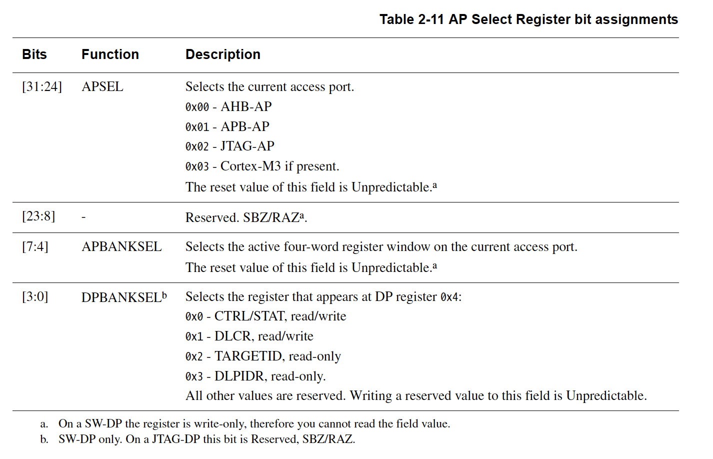
The most common type of Access Port is known as the MEM-AP which exposes an interface to different Memory buses available on a given ARM chip. On ARM Cortex-M, the MEM-AP which is typically accessed is known as the AHB-AP. The default APs that are selected can be found in the APSEL part of the DP AP Select Register1:
AHB-AP
The Advanced High-performance Bus (AHB) is a bus present on ARM devices that interconnects the memory and peripherals present on the MCU. The AHB-AP exposes access to this bus via several registers. The most common registers used in the AHB-AP are:
-
Control/Status Word register (
CSW) Used to configure the rules to be used when performing a memory access on the AHB. -
Transfer Address Register (
TAR) Used to control the address that will be accessed -
Data Read/Write register (
DRW) Depending on the access, contains the data to write to or read from theTAR
Extensive details about how to access the register set can be found in the ARM Debug Interface Specification2
Debug Port External Connection Options
The DAP spec defines three different protocols which can be used to expose an interface from the Debug Port to the outside world. They are:
-
JTAG Debug Port (JTAG-DP) - Based on the IEEE 1149.1 Standard for Test Access Port (
TAP). AJTAGinterface is exposed in pretty much any piece of silicon and was standardized in 1990 with several revisions added over the years. This debug interface requires the MCU expose at least 4 pins and one optional pin (DBGTRSTn). At its core, the protocol operates on a sequence of shift registers and a fairly complex state machine to push data in / get data out -
Serial Wire Debug (SWD) Port (SW-DP) -
SWDwas designed to reduce the number of physical pins that need to be exposed. MCUs have a small number of pins available and reducing the pin count needed for debugging means there are more GPIOs free for external sensors or that a smaller footprint package can be used. One pin,SWDIO, is used for input/output and the otherSWCLKis used for clocking data in and out. Sampling ofSWDIOis performed on the rising edge of the clock -
Serial Wire/JTAG Debug Port (SWJ-DP)
SWJ-DPis the best of both worlds and exposes an interface whereJTAGorSWDcan be used. The pins are carefully assigned between the two protocols so a negotiation can take place to select the protocol that is in use. This is the configuration you will see exposed on most MCUs because the user can then chose to use either protocol depending on their needs
Debug Probes
The next step is getting a computer to talk to the MCU. Typically another piece of hardware (often referred to as an “interfacing MCU”) will be used to map from the SWD or JTAG connection to a USB protocol that can talk to the computer. Sometimes the interface will be provided via an external dongle and other times via an integrated IC on the development board being used. If you are designing your own development board, it’s always a good idea to expose these debug pins to an external header to keep your options open.
Debug Probe Options
There are quite a few interfacing options you will see depending on the ARM MCU, IDE, and development kit you are using. Some of the most popular are:
-
Future Technology Devices International (FTDI)’s FT Series chips which expose a bridge between USB and the raw signal lines they are connected to. The same chip is also very popular for exposing a UART connection. They are fairly cheap and expose a USB interface, know as The Multi Protocol Synchronous Serial Engine (
MPSSE), which can be used for issuingJTAGorSWDtransactions (and other serial protocols) - CMSIS-DAP3 4 A standardized protocol for interfacing with the ARM Debug Access Port. ARM maintains an open source implementation of the specification know as DAPLink5. This image is flashed on an interfacing MCU where one side is connected to the pins of the MCU being debugged and the other side exposes a USB connection which communicates using USB HID commands. The nice part about this standard is that it can talk JTAG & SWD but the protocol does not need to be implemented on the computer. Additionally since almost any modern computer has support for HID, no additional USB drivers are needed. Many development kits come with a CMSIS-DAP pin compatible MCU available that can easily be re-flashed. For example, the LPC-Link26 found on a lot of NXP dev boards does this.
-
SEGGER J-Link Debug Probe7 A proprietary cross-platform debug probe that bridges USB to
JTAGorSWD. There are many different form factors available and SEGGER also has firmwares available to convert a lot of other debug probes to be J-Link compatible - ST-Link8 - A proprietary debug probe maintained by STMicroelectronics. There has been three iterations of the hardware, the latest of which is known as STLINK-V3
Desktop Software to Interface with Debug Probe
Once you have selected a debug probe, the next step is choosing what software on the computer to use to communicate with the probe.
There are numerous options available but an overwhelming majority of the software stacks available will expose a gdbserver interface which exposes the “GDB Remote Serial Protocol”9 on one side and talks the necessary debug probe protocol to the interfacing MCU on the other. Even if you are using an Eclipse based IDE (i.e NXP’s MCUXpresso, STM32CubeIDE, TrueSTUDIO, WICED-Studio IDE, etc), the debug interface is usually leveraging a gdbserver behind the scenes.
When selecting the software to use, the other item you want to look at is its board support. If the MCU in use has an internal micro flash, many of these probes also come with support for programming that flash so you can easily load new programs on the MCU.
GDB Server Options
The actual GDB server used is usually based on the debug probe selected. Some of the common choices are:
- pyOCD10 A Python-based open source implementation compatible with CMSIS-DAP and ST-Link debug probes. The project is maintained by ARM. This is my favorite gdbserver at the moment. If you want to understand more about the ARM Coresight internals, reading through the code itself is actually a great reference and being open source the framework can be easily extended to support a variety of use cases.
-
openOCD11 A C-based open source
gdbserverimplementation for a wide array of debug probes. The project probably supports the widest array of debug probes out of any project available (you can runopenocd -c interface_listto see) including FTDI, CMSIS-DAP, J-Link and about 17 other adapters. The project dates back to 2005 and while it has support for a wide array of parts I have found it to be a bit flaky to use for projects over the years. -
SEGGER JLinkGDBServer12 A proprietary
gdbserverdistributed as a binary. Has support for an impressive amount of devices. (You can find the list at<SEGGER JLink install path>/JLinkDevices.xml). I’ve found it to be quite reliable for debugging but when there are issues, things can be quite painful to fix without being able to see the source - texane/stlink13 An open source implementation of the ST-Link Debug Probe protocol. This project is independently maintained and not affiliated with ST.
- Proprietary GDB Servers used with different IDEs such as PEMicro GDB Server14, NXP LinkServer/Redlink and ST-LINK_gdbserver15.
Extending Debug Probe Software
RTOS Awareness
Features like RTOS Awareness – the ability to see all the tasks currently active on an MCU when you run info threads or view a task list in Eclipse – needs to be implemented on the gdbserver side. When a GDB client connects to a server, it will ask the server for the thread list. If the server can’t resolve the thread list, it will only show the stack trace for the active task.
The RTOS awareness implementations all wind up looking pretty similar. The GDB Remote Serial Protocol has a message, qSymbol, which can be used to ask the client to look up the address for a given symbol (i.e pxCurrentTCB would be a symbol you’d need to look up the address of in order to implement a FreeRTOS plugin). The server will look up the symbols it needs to uncover the Thread Control Block (TCB) for all the tasks in the system. Once it has the list, the gdbserver will recover the state of each thread by issuing reads to the memory of the MCU. Sometimes to aid in the recovery of this information an RTOS will export special symbols to expose offsets of TCB info. (i.e Zephyr16)
Conveniently, many of the GDB Server options expose APIs for implementing thread awareness. The ones I am aware of and have implemented RTOS plugins with include:
- OpenOCDs RTOS plugin17 A C-based RTOS-plugin API
- SEGGER GDB Server RTOS plugin SDK18 You have to request access but the API is also in C. If you look at the way the OpenOCD plugin works the SEGGER based API is extremely similar.
- pyOCD RTOS plugin19 The API is in Python but similarly structured to the other two C based APIs
SEGGER Open Flashloader / Custom flash loaders
A ton of MCUs these days allow one to execute code from external flash parts. Very rarely will the debug probe software have a pre-existing flash loader for a custom configuration like this. SEGGER conveniently has an API to implement a Custom Flash Loader.
The way it works is you provide micro-code that is flashed into RAM to initialize, read, erase, and write to the flash part of interest. The SEGGER JLinkGDBServer will just jump to these functions to perform the operations on the external flash. I’ve implemented a few of these and while it can be a convenient tool to have, developing these plugins can be quite challenging as this code runs before the debugger starts. So a failure will not drop out to a breakpoint you can look at. The “best” way to debug these plugins is to sprinkle messages in RAM which can be read post-mortem.
The Desktop Debugger
All of the pieces we’ve mentioned stack together and make up “the debugger”.
There a few common interfaces to the stack:
- a GDB Cli Client that you would launch by running a command like:
arm-none-eabi-gdb-py --eval-command="target remote localhost:<remote port>" --symbols=<ELF>
- An Eclipse based GUI that has different views you can use to inspect variables or see memory
- VSCode Plugins2021 that interfaces with GDB and let’s you hover over and view variables
Tracing a Transaction
Now that we understand a bit about the software stack in play. Let’s trace through a transaction to better understand what’s happening end to end.
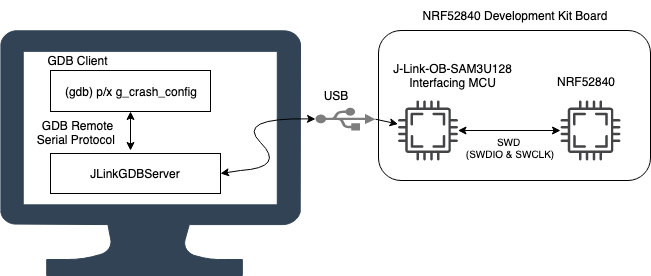
For this setup we will use:
- A nRF52840-DK running the blinky demo application from our MPU blog post
- A saleae logic analyzer22
Debug Path
The end to end path of our debug setup looks like this:
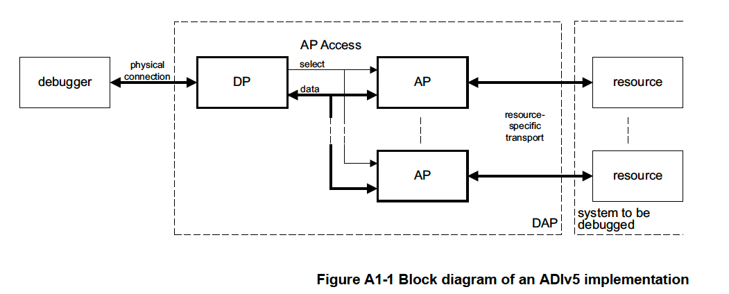
The following image from the ARM Debug Interface Architecture manual2 captures what the path looks like inside the NRF52840. The “physical connection” in this case is the SWD path in the image above.
Prepping the board
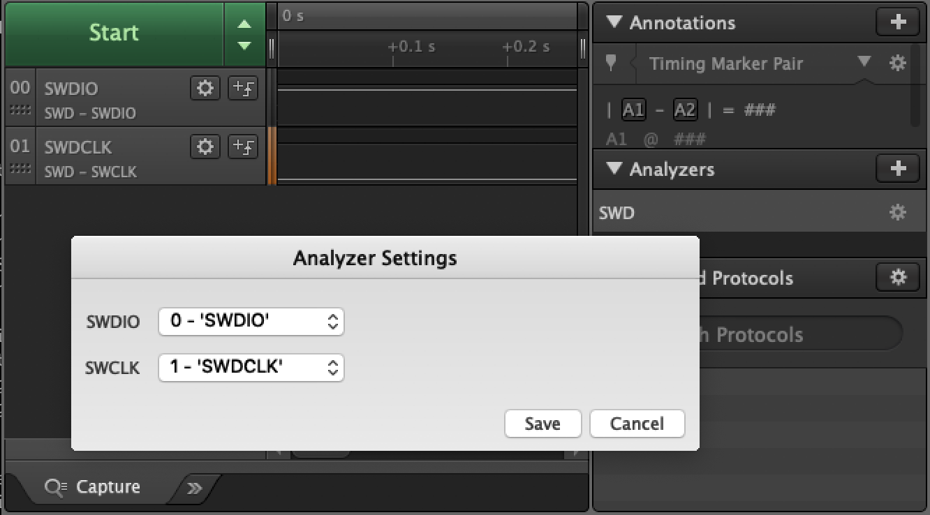
On the nRF52840-DK board I see P18 is labeled as “Debug In”. Looking at the schematics23, I can easily see the pinout:
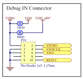
I attached the Saleae ground to Pin 9, wire 0 to SWDIO at P18 Pin 2, and wire 1 to SWDCLK at P18 Pin 4.
In the Saleae Logic App, I then enabled these 2 pins, and added the SWD analyzer:
Flashing the App
For the purposes of this experiment we will look at what is happening with SEGGER J-Link. The invocation I used was:
JLinkGDBServer -if swd -device nRF52840_xxAA -speed 500
I manually set the speed to a low value just to play it safe. You usually want the sampling rate to be at least 4x faster than the maximum frequency being measured. So if SWDCLK is running at 500kHz, we want to sample with a rate of at least 2 MegaSamples / second or greater.24 However, the faster we sample, the better our timing resolution will be.
To flash the device and attach to the GDB server, I used my personal favorite debug client, the GDB CLI:
arm-none-eabi-gdb-py --eval-command="target remote localhost:2331" --ex="mon reset" --ex="load" --ex="mon reset" --se=_build/nrf52840_xxaa.out
Capturing a Trace
Now that we have the Saleae, let’s trace a read transaction. The steps we will walk through below would work for any other type of transaction you want to investigate as well:
Let’s read the g_crash_config variable and see what happens
First, we need to halt GDB by running CTRL-C, then “Start” a capture within the Saleae Logic App and run this in GDB:
(gdb) p/x g_crash_config
$1 = 0x0
We can determine the address and size of the read that needs to take place by inspecting the variable in gdb:
(gdb) p sizeof(g_crash_config)
$3 = 4
(gdb) p &g_crash_config
$4 = (int *) 0x20000108 <g_crash_config>
The first transaction we see over the wire gets decoded by the Saleae as follows:
![]()
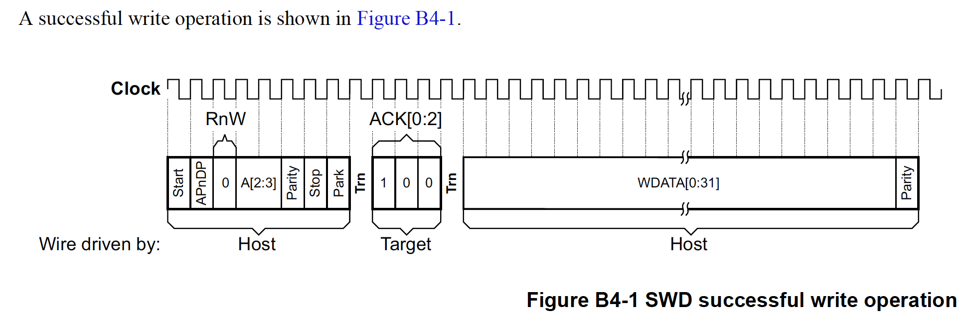
We see it’s an ABORT Debug Port write. This is a good operation to run before issuing any transactions because it will reset the state of the current AP and put the debugger into a known state. If you wanted to decode the transaction without the Saleae analyzer, the ADIv5 reference manual2 provides the information needed. The structure for a write operation looks like this:
Saleae CSV Trace
The Saleae analyzer also lets us export the analysis as a CSV file. Let’s walk through the transactions that we see. I’ve added some observation notes inline below:
Time [s], Analyzer Name, Decoded Protocol Result
//
// Write to the AP Abort Register (ABORT) to reset state
//
3.235528170000000,SWD,Request  DebugPort Write ABORT
3.235544810000000,SWD,Turnaround
3.235546840000000,SWD,ACK OK
3.235552900000000,SWD,Turnaround
3.235554950000000,SWD,WData 0x0000001E reg ABORT bits ORUNERRCLR=1, WDERRCLR=1, STKERRCLR=1, STKCMPCLR=1, DAPABORT=0
3.235621490000000,SWD,Data parityok
3.235623550000000,SWD,Trailing bits
//
// Write to the SELECT register. This is used to target the AP of
// interest. You can discover all the available APs by walking through
// the "ROM Table" (more details in the ADIv5 Specification). Per the
// Coresight specification, we know when APSEL=0x0, the AP selected
// is AHB-AP
//
3.235647510000000,SWD,Request  DebugPort Write SELECT
3.235664140000000,SWD,Turnaround
3.235666160000000,SWD,ACK OK
3.235672230000000,SWD,Turnaround
3.235675260000000,SWD,WData 0x00000000 reg SELECT bits APSEL=0x00, APBANKSEL=0x0, PRESCALER=0x0
3.235741780000000,SWD,Data parityok
3.235746540000000,SWD,Request  AccessPort Write CSW
3.235763170000000,SWD,Turnaround
3.235765200000000,SWD,ACK OK
3.235771260000000,SWD,Turnaround
//
// We are accessing a AHB-AP of type MEM-AP. The CSW register is
// written to in order to configure what type of access will be
// performed. One interesting setting is AddrInc which is used to
// control whether or not the access address is automatically
// incremented after a read.
//
3.235774290000000,SWD,WData 0x23000012 reg CSW bits DbgSwEnable=0, Prot=0x23, SPIDEN=0, Mode=0x0, TrInProg=0, DeviceEn=0, AddrInc=Increment single, Size=Word (32 bits)
3.235840750000000,SWD,Data parityok
//
// The Transfer Address Register (TAR) is now programmed with
// address of interest. It's close to the address we are trying to
// read (0x20000108) but interestingly does _not_ match
//
3.235844790000000,SWD,Request  AccessPort Write TAR
3.235861420000000,SWD,Turnaround
3.235863450000000,SWD,ACK OK
3.235869510000000,SWD,Turnaround
3.235872550000000,SWD,WData 0x20000100 reg TAR
3.235939040000000,SWD,Data parityok
//
// A request to read the data via the Data Read/Write Register (DRW)
// is finally issued. This will return the data at address 0x20000100
// and then increment the address in the TAR by 1 word so the next read
// would return 0x20000104
//
3.235943310000000,SWD,Request  AccessPort Read DRW
3.235959910000000,SWD,Turnaround
//
// Data is not ready yet so a ACK WAIT is returned
//
3.235961940000000,SWD,ACK WAIT
3.235971240000000,SWD,Request  AccessPort Read DRW
3.235987840000000,SWD,Turnaround
//
// Our read request has been ACKd. Per the ADIv5 documentation
// the read request has "posted" which means that
// "the result of the access is returned on the next transfer.
// This result can be another AP register read, or a DP register
// read of RDBUFF." This means the data in this transaction
// should be discarded
//
3.235989860000000,SWD,ACK OK
3.235995920000000,SWD,WData 0x00000000 reg DRW
3.236062190000000,SWD,Data parityok
3.236068440000000,SWD,Request  AccessPort Read DRW
3.236085030000000,SWD,Turnaround
3.236087060000000,SWD,ACK OK
//
// The actual value of the data at 0x20000100.
//
3.236093120000000,SWD,WData 0x00000000 reg DRW
3.236163440000000,SWD,Data parityok
3.236169630000000,SWD,Request  AccessPort Read DRW
3.236186220000000,SWD,Turnaround
3.236188250000000,SWD,ACK OK
//
// The actual value of the data at 0x20000104.
//
3.236194310000000,SWD,WData 0x00000000 reg DRW
3.236260570000000,SWD,Data parityok
3.236266750000000,SWD,Request  AccessPort Read DRW
3.236283360000000,SWD,Turnaround
3.236285380000000,SWD,ACK OK
//
// The actual value of the data at 0x20000108. (The address we
// wanted to read in the first place!)
//
3.236291450000000,SWD,WData 0x00000000 reg DRW
3.236357710000000,SWD,Data parityok
3.236363900000000,SWD,Request  AccessPort Read DRW
3.236380490000000,SWD,Turnaround
3.236382520000000,SWD,ACK OK
//
// The actual value of the data at 0x20000110.
//
3.236388580000000,SWD,WData 0x3910E7EF reg DRW
[...]
// In the actual trace we see another 12 reads performed
// bringing the total bytes read by the debugger to 16 bytes.
That’s interesting, it seems like the debugger is caching 16 bytes of data. If we “Start” a trace while reading in this memory range we will see no SWD transactions get issued! To test it out, start the Saleae trace again and run
(gdb) p/x *(uint32_t[16]*)0x20000100
$10 = {0x0, 0x0, 0x0, 0x3910e7ef, 0xe0111c06, 0x1c26390c, 0x3908e00e, 0xe00b1c2e, 0xe0091f09, 0xd40d1e7f, 0x42b3680e, 0x1d09d104, 0xd1f71f12, 0xbdf22000, 0x60019806, 0x60069807}
This means the JLinkGDBServer must be caching results and not always issuing requests to the actual MCU.
If we try to read 17 bytes we will see a new transaction gets issued with TAR starting at 0x20000140.
For reference, I’ve included trace here. The original trace was in the same directory.
Closing
We hope this post gave you a better understanding of the technology that makes up the Cortex-M ARM debug stack and that in the future when you run into a debugger issue you have a better idea of where to start looking for issues!
Future topics we’d love to delve into related to debuggers include the Embedded Trace Macrocell (ETM) and Data Watchpoint and Trace (DWT) peripherals, as well as implementing thread awareness and flash loader plugins.
Are there other topics you’d like us to cover? Or are there topics in this article you’d love to see more details on? Just let us know in the discussion area below!
See anything you'd like to change? Submit a pull request or open an issue on our GitHub
Useful Reference Links
 Chris Coleman is a founder and CTO at Memfault. Prior to founding Memfault, Chris worked on the embedded software teams at Sun, Pebble, and Fitbit.