Fix Bugs and Secure Firmware with the MPU
On a computer when an application dereferences a NULL pointer or tries to access kernel memory we can catch it pretty easily thanks to the features provided by the MMU on the chip.
For embedded development on MCUs, we aren’t always so lucky. A bad memory access from a task responsible for reading an accelerometer could corrupt a buffer being used elsewhere in the system to update a display! Fortunately, not all hope is lost …
Many ARM MCUs implement an optional unit, known as the Memory Protection Unit (MPU), which lets you control how regions of memory are accessed. In this article, we will deep dive into the unit and walk through a few practical examples of how it can be used to prevent bad memory accesses and security exploits on Cortex-M devices.
If you’d rather listen to me present this information and see some demos in action, watch this webinar recording.
Table of Contents
A Little History
The MPU made its debut as an optional feature of the ARMv7-M architecture and appears in many Cortex-M3, Cortex-M4, and Cortex-M7 based processors. A very similar implementation was also added as a feature to the ARMv6-M architecture (a simpler & lower power alternative derived from ARMv7-M) which some Cortex-M0+ processors implement. Newer architectures (such as ARMv8-M used on the Cortex-M33) implement an improved version of the MPU but for the purposes of this article we will focus on the ARMv6/7-M variant.
Overview of MPU functionality
At its core, the MPU lets you control the access to regions in “the system address map” (see section in reference manual). This includes memory areas like internal flash, SRAM, peripherals, and memory mapped devices (i.e external RAM/flash).
The MPU also allows for an application level programmers’ model to be implemented in software. When an ARM Cortex-M based device is running code outside of an exception handler, it’s referred to as running in thread mode. When in thread mode, code can be running as Privileged or Unprivileged (configured via the special-purpose CONTROL register). The MPU will let you change what memory regions can be accessed based on this setting. For example, while in Unprivileged thread mode, all peripheral accesses (like reading from an external flash) could be disabled. It is common to use this model when an MCU is running untrusted code (i.e third party applications). In this manner, the code can be sandboxed such that the third party app can’t corrupt or crash the system or steal data. This configuration setting is known as access permissions (AP) and can be used to:
- disable all read & write accesses for privileged and/or unprivileged code.
- disable unprivileged writes
- make areas read-only for privileged and/or unprivileged code.
Additionally, the MPU let’s you configure if a region of memory can be executed from using the eXecute Never capability (XN). In a previous article, we discussed how different regions of memory will hold code (text) and data. Sometimes arbitrary data (like a string from a printf() statement) can look like valid ARM instructions. A classic security vulnerability would be to find a way to execute this data as code, escalate privileges and harm the system or steal information. We’ll explore this concept in more detail below.
MPU registers
The MPU is configured using just five registers! A great way to build an understanding for how the unit works is to read the descriptions for these registers. They are well-documented in the Register support for PMSAv7 in the SCS section of the ARMv7-M reference manual. Let’s walk through the highlights here, go over typical configurations and discuss common mistakes made.
MPU Type Register
MPU_TYPE - Address 0xE000ED90 register bit assignments:
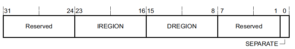
This register is present regardless of whether or not the MPU was implemented on the Cortex-M device being used. This is pretty nice because it allows us to dynamically determine at runtime or via a GDB Python script whether or not an MPU is present and use it. The only field of interest here is DREGION which reveals the number of MPU regions which were implemented. A value of 0 for DREGION indicates the MPU was not implemented.
MPU Control Register
MPU_CTRL - Address 0xE000ED94 register bit assignments:
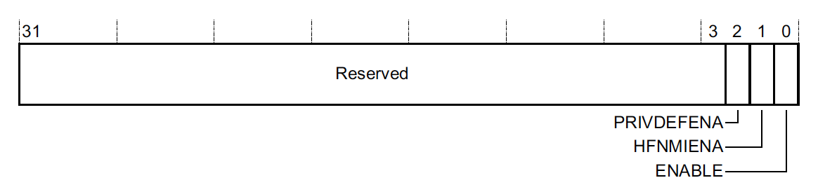
This register is how we actually enable the MPU. Until the ENABLE bit is set, the MPU configuration in other registers have no effect.
PRIVDEFENA controls whether or not code running in Privileged thread mode can access the default memory map. If the bit is set to 0, any access not explicitly enabled via the MPU will result in a fault when the ENABLE bit is set. In a typical configuration using the MPU, this bit will be set to 1.
HFNMIENA controls whether or not the MPU is active when running from fault handlers. Since most fault handler implementations end in a reboot, I usually leave this bit set to 0 so that it’s easier to collect a full coredump of the memory state at the time of crash. This can greatly facilitate offline debug of why the issue which triggered the Memory Management Fault happened in the first place!
MPU Region Number Register
MPU_RNR - Address 0xE000ED98 register bit assignments:
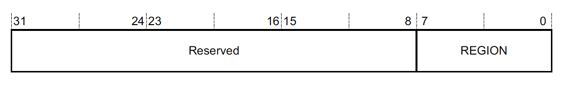
As we saw in the MPU_TYPE register above, the MPU is broken into a certain number of configurable-regions. The M0+, M3 & M4 can support up to 8 regions when the MPU is implemented and the M7 can support up to 16! The REGION field is used to select the active region we want to read or update. Once the region is selected, we can read or write MPU_RBAR & MPU_RASR to see the configuration and make changes.
Caution It’s worth mentioning that there is a priority scheme to these regions. If the same memory range is covered in multiple MPU regions, the configuration in the highest REGION number will be applied. So for example, if REGION 0 turns off access to the first 32kB of RAM for Unprivileged mode but REGION 1 makes the same RAM region read-only, REGION 1 settings will take precedence. This means code running in Unprivileged mode will be able to read the memory.
Note The default memory map enabled with the PRIVDEFENA mentioned above has a priority of -1 and so it will be overridden by any configurations made in these regions.
MPU Region Base Address Register
MPU_RBAR Address 0xE000ED9C register bit assignments:
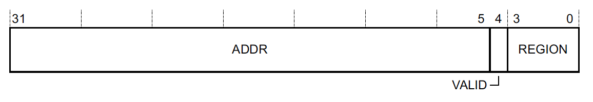
This register is used to control the starting address (aka the base address) that we want to cover with the region selected in MPU_RNR. For example, if we wanted to protect the address range starting at the beginning of a SRAM range (i.e 0x20000000) using REGION 0, we would first set MPU_RNR to 0 and then set MPU_RBAR to 0x20000000)
To reduce the number of writes needed to change the configuration, the VALID bit can be set to 1 and the REGION field can be set to change the value of MPU_RNR and apply the write to a different region. For example, if we wanted to set REGION 7 to have a base address of 0x20000000, we could write 0x20000000 | 0x1 << 4 | 0x7 == 0x20000017 to MPU_RBAR. If we then read MPU_RNR, we would see its value is now 0x7.
Caution You may have noticed the address only occupies 27 bits and the bottom 5 bits were repurposed. What if we want to protect an address that starts with a base of 0x20000002? You can’t! The minimum region size is implementation defined but is usually 32 bytes. The actual size supported can usually be looked up in the reference manual for the specific MCU being used. Alternatively, it can also be dynamically determined by writing 0xFFFFFFE0 to MPU_RBAR and reading the value back. The number of trailing zeros will reveal the minimum supported alignment and consequently the minimum region size. For example, reading a value of 0xFFFFFF80 would reveal bits 5 and 6 can’t be set so the minimum size supported is 2^7 (128) bytes.
MPU Region Attribute and Size Register
MPU_RASR - Address 0xE000EDA0 register bit assignments:
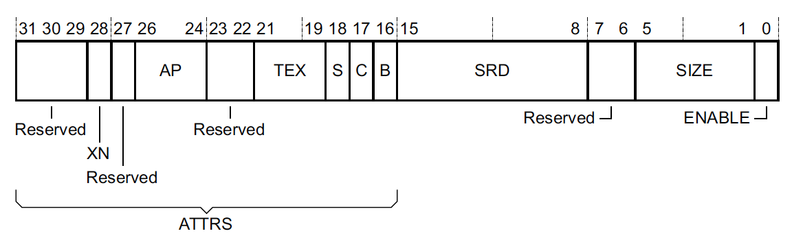
This is the register where nearly all of the MPU configuration magic actually happens. The ENABLE bit controls whether or not the region is active (when the MPU itself has been enabled by setting the ENABLE bit in MPU_CTRL).
The configuration can be broken down into four main parts:
1. Memory Type, Cacheability & Shareability
This config is comprised of the TEX (Type Extension Mask), C (Cacheable), B (Bufferable), & S (Shareable) fields. More details about each memory attribute can be found in the Summary of ARMv7 memory attributes of the ARMv7-M reference manual. Typically, these settings do not matter much for a single core Cortex-M implementation. I usually follow the recommendations in the table below from here:
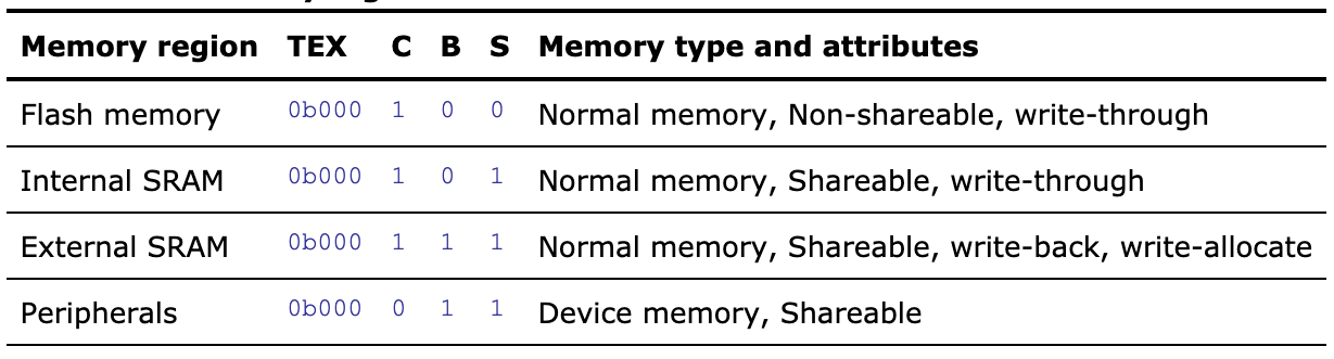
If you are using a more complex Cortex-M setup (like a Cortex-M7 with a cache), the vendor data sheet may have a section with better recommendations.
2. Access permissions & Execute Never encoding
This part is comprised of the AP (Access Permissions) fields used to control the rules around how the region can be accessed:
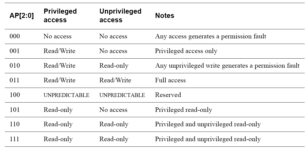
There is also the XN (Execute Never) field, used to control whether or not the processor can fetch instructions from this region. If the XN bit is set, an instruction fetch from the region will cause a fault.
Caution Even if the XN bit is not set, a fault could still occur on instruction fetch if read access is disabled in the AP config for the region we are trying to fetch an instruction from.
3. Region Size
Indicates the size the region spans over, where the size is 2 ^ (SIZE field + 1). The start is the address provided as the base address in MPU_RBAR. So for example if the base address is 0x20000000 and the SIZE field is 0b10000 == 16, the MPU region will cover 0x20000000 to 0x20000000 + 2^(16+1) = 0x20020000.
Caution: The SIZE selected here must be aligned with the base address provided in MPU_RBAR. Otherwise, you will wind up covering a region that is different than expected since the base ADDR is always naturally aligned with the SIZE. For example, if we had set ADDR above to 0x20001000, the same region will still wind up being covered because 0x1000 would be masked out under the hood!
4. Sub-Region Disable
The SRD (Sub-Region Disable) field is a bitmask that lets you turn off the MPU region for 1/8 units of the region selected. The SIZE of the region must be greater than 256 bytes for this to have any effect.
For a complex embedded device, it’s easy to start to run low or out of available MPU Regions. This field provides a clever way to cover more things. For example, imagine you want to protect the first and last 32kB blocks of a 256kB RAM the same way. You could enable a MPU region that covers all 256kB but set the SRD field to 0x7e so only the first and last 1/8 blocks (each 32kB) in the MPU region are active.
MPU Alias Register Support
Up to this point, the registers we have described are the same for the ARMv6-M & ARMv7-M MPU implementations. The ARMv7-M re-aliases the MPU_RBAR & MPU_RASR registers 3 times in a sequential address range. While not necessary to use, this can be useful for initialization because you can create a configuration array that is 32 bytes and then program four regions at once with just a stream of word writes.
MPU Usage Examples
Now that we have a better grasp of what an MPU does and how to configure it, let’s try a couple real world examples. For the purposes of this demo, I am using a nRF52840 DK and running the blinky demo application compiled at examples/peripheral/blinky/pca10056/blank/armgcc in the v15.2 SDK. However, you should be able to run similar code snippets on pretty much any ARMv6-M or ARMv7-M processor with an MPU!
The examples which follow will walk through building up a collection of MPU region configurations and example crashes but you can also look at the code in it’s entirety here which is a drop-in replacement for the blinky main.c located at examples/peripheral/blinky/main.c in the SDK.
NOTE For convenience, the code makes use of a couple GCC extensions, notably some function attributes and binary constants but could easily be modified to target other compilers as well.
Examine NRF52 MPU Implementation
Let’s read the MPU_TYPE register from GDB to sanity check that it has a MPU implemented and determine the number of regions available! As mentioned above this is in the 8 bit DREGION field
(gdb) p/x (*(uint32_t*)0xE000ED90>>8)&0xff
$1 = 0x8
Great, we have 8 regions to work with!
Now let’s check the minimum region size supported. As described in the MPU_RBAR section above this can be resolved by setting bits 32-5 to 1. If all the bits remain set, it means the smallest possible size of 32 bytes is supported. We can check this out in GDB as well and confirm the NRF52 supports a minimum region size of 32 bytes:
(gdb) set *(uint32_t*)0xE000ED9C=0xffffffe0
(gdb) p/x *(uint32_t*)0xE000ED9C
$3 = 0xffffffe0
Enable MemManage Fault Handler
Let’s override the default MemManage fault handler for the purposes of our example to just trigger a breakpoint. That way GDB will halt as soon as
a MemManage Fault is hit and we can investigate further.
// The NRF52 fault handlers can be overridden because they are declared as weak
// Let's override the handler and insert a breakpoint when it's hit
__attribute__((naked))
void MemoryManagement_Handler(void) {
  __asm("bkpt 1");
}
The MemManage fault is off by default. (When it’s off an MPU fault will immediately escalate to a hardfault). You will need to add the following code somewhere during init to enable the exception:
  // Let's set MEMFAULTENA so MemManage faults get tripped
  // (otherwise we will immediately get a HardFault)
  volatile uint32_t *shcsr = (void *)0xE000ED24;
  *shcsr |= (0x1 << 16);
Catch Stack Overflows with the MPU
For illustrative purposes, let’s add a simple recursive function to main.c. We’ll also disable optimizations in all our examples so it’s easier to step through the code in a debugger.
__attribute__((optimize("O0")))
int recursive_sum(int n) {
  if (n == 0) {
    return 0;
  }

  return n + recursive_sum(n-1);
}
From our main loop let’s call recursive_sum(600). If you compile and run the application, you should see the LEDs blink in a loop. Things appear to be working. Let’s use MPU Region 0 just to be sure we aren’t overflowing our stack.
The NRF52 SDK defines a linker script variable, __StackLimit, which can be used to determine where the end of the stack is. We’ll set up a 64 byte MPU region at the bottom of the stack so we can catch a stack overflow as it is happening. Based on what we learned above, the configuration settings we need to add to our code will look something like:
  volatile uint32_t *mpu_rbar = (void *)0xE000ED9C;
  volatile uint32_t *mpu_rasr = (void *)0xE000EDA0;

  extern uint32_t __StackLimit;
  // align base address to nearest 64 byte boundary
  // because it needs to match SIZE
  uint32_t mask = 64 - 1;
  const uint32_t base_addr = ((uint32_t)&__StackLimit + mask) & ~mask;

  // Let's set the base_address and use the 'VALID'
  // bit to make sure region 0 is active in 'MPU_RNR'
  *mpu_rbar = (base_addr | 1 << 4 | 0);

  // MPU_RASR settings:
  //  AP=0b000 because we don't want to allow _any_ access
  //  TEXSCB=0b000110 because the Stack is in "Internal SRAM"
  //  SIZE=5 because we want a 64 byte MPU region
  //  ENABLE=1
  *mpu_rasr = (0b000 << 24) | (0b000110 << 16) | (5 << 1) | 0x1;
Finally, let’s activate the MPU:
  // Finally, activate the MPU and default memory map (PRIVDEFENA)
  volatile uint32_t *mpu_ctrl = (void *)0xE000ED94;
  *mpu_ctrl = 0x5;
If we have a debugger attached, we should hit the breakpoint we set:
(gdb) c
Continuing.

Program received signal SIGTRAP, Trace/breakpoint trap.
MemoryManagement_Handler () at ../../../main.c:20
20    __asm("bkpt 1");
When a MemManage fault is hit there are a couple registers that are very helpful to look at.
The first is the MemManage Status Register (MMFSR) - 0xE000ED28:
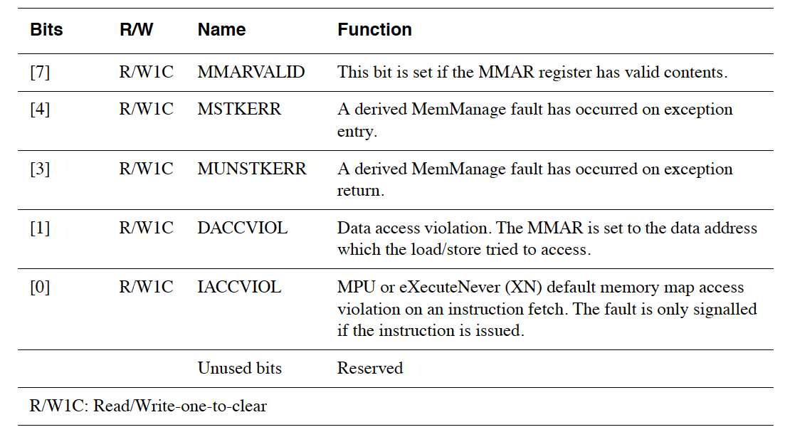
The second is the MemManage Fault Address Register (MMFAR) located at 0xE000ED34 which contains the address of the access which triggered the fault provided MMFSR.MMARVALID is set.
Let’s look at this information in GDB and compare it to the bottom of the stack, &__StackLimit.
(gdb) p &__StackLimit
$1 = (uint32_t *) 0x2003e000
(gdb) p/x *(uint32_t*)0xE000ED28
$2 = 0x92
(gdb) p/x *(uint32_t*)0xE000ED34
$3 = 0x2003e038
We see our MMARVALID is set so we know the fault took place when the address 0x2003e038 was accessed. This is directly above the bottom of our stack, 0x2003e000, at the top of the 64 byte MPU region we allocated! So our deep recursive routine is overflowing. Even though things appeared to be working we were silently corrupting the memory below our stack. This would almost certainly cause subtle issues in the future when the linker placed a variable in that area or we moved a heap to that region.
Catch Writes To Flash
On ARM processors, 0x0 is a valid address. 0x00000000-0x1FFFFFFF is specified as a Code region and usually maps to internal flash. On most processors writes to this address range are a no-op. This means a NULL pointer dereferences and write can go uncaught. We can try it out on our MCU by adding a function that looks something like this:
__attribute__((optimize("O0")))
void invalid_write_to_flash(void) {
  volatile uint32_t *bad_pointer = (void *)0x0;
  *bad_pointer = 0xdeadbeef;
}
Running this in the main loop on the NRF52 blinky app, we see the LEDs happily blinking.
To help us catch nefarious NULL-pointer dereference bugs, let’s extend our example app and use MPU Region 1 to make the flash space read-only. For the NRF52840, the code we need to add will look something like this:
  // The NRF52840 internal flash is 1MB and starts at address 0x0
  // No need to mask the address since it's fixed and 1MB aligned
  base_addr = 0x0;
  // Let's use the 'VALID' bit to select region 1 in 'MPU_RNR'
  *mpu_rbar = (base_addr | 1 << 4 | 1);

  // MPU_RASR settings for flash write protection:
  //  AP=0b110 to make the region read-only regardless of privilege
  //  TEXSCB=0b000010 because the Code is in "Flash memory"
  //  SIZE=19 because we want to cover 1MB
  //  ENABLE=1
  *mpu_rasr = (0b110 << 24) | (0b000010 << 16) | (19 << 1) | 0x1;
Now when we run the example with a debugger attached we see clearly where the bad access took place and can fix the problem!
MemoryManagement_Handler () at ../../../main.c:26
26    __asm("bkpt 1");
(gdb) p/x *(uint32_t*)0xE000ED28
$1 = 0x82
(gdb) p/x *(uint32_t*)0xE000ED34
$2 = 0x0
(gdb) bt
#0  MemoryManagement_Handler () at ../../../main.c:26
#1  <signal handler called>
#2  0x000002fe in invalid_write_to_flash () at ../../../main.c:19
#3  0x00000358 in main () at ../../../main.c:81
(gdb) frame 2
#2  0x000002fe in invalid_write_to_flash () at ../../../main.c:19
19    *bad_pointer = 0xdeadbeef;
Catch Execution of Data Array As Code
Now let’s look at an example where an array of data is getting executed as if it’s valid code. In this example, we just so happen to have an array of “random” data that has a valid SVC instruction within it. The SVC instruction is used for switching between privileged and unprivileged mode so on a real world system that runs third party code this could be the start of a serious security exploit!
// An array of data that "happens" to have a pattern of valid
// ARM instructions.
//
// Note: We are aligning the data along a boundary that matches its
// size for simplicity in our MPU configuration example
static const uint16_t s_data[64] __attribute__((aligned(128))) = {
  0xbf00, // nop
  0xbf00, // nop
  0xdf00, // svc 0
  0x4770, // bx lr
};

__attribute__((optimize("O0")))
void execute_data_array_as_code(void) {
  uint32_t func_addr = (uint32_t)&s_data[0];
  // bit[0] of a function pointer must be set to 1 per per
  // "ARMv7-M and interworking support" section of reference manual
  func_addr |= 0x1;

  // perform a read/write
  s_data[5] |= 0xabab;

  // execute the array like it's a function
  void (*data_as_function)(void) = (void *)func_addr;
  data_as_function();
}
On the NRF52840, the default SVC_Handler is a while (1) loop so calling execute_data_array_as_code() wedges the system in an infinite loop in an interrupt which isn’t great either! Let’s guard the data region with MPU Region 2 and set the Execute Never (XN) bit to intercept this kind of attack! The MPU configuration will look something like:
  // The s_data struct is 128 bytes in size and is already 128 byte aligned
  base_addr = (uint32_t)&s_data[0];
  // Let's use the 'VALID' bit to select region 2 in 'MPU_RNR'
  *mpu_rbar = (base_addr | 1 << 4 | 2);

  // MPU_RASR settings for flash write protection:
  //  XN=1 to block _any_ attempts to execute the region as code
  //  AP=0b011 to allow full read/write access to the region
  //  TEXSCB=0b000110 because the Stack is in "Internal SRAM"
  //  SIZE=6 because we want to cover 128 bytes
  //  ENABLE=1
  *mpu_rasr =
      (0b1 << 28) | (0b011 << 24) | (0b000110 << 16) | (6 << 1) | 0x1;
Let’s run the code with a debugger and see what we get this time:
MemoryManagement_Handler () at ../../../main.c:53
53    __asm("bkpt 1");
(gdb) p/x *(uint32_t*)0xE000ED28
$3 = 0x1
(gdb) bt
#0  MemoryManagement_Handler () at ../../../main.c:53
#1  <signal handler called>
#2  0x20000000 in s_data ()
#3  0x00000318 in execute_data_array_as_code () at ../../../main.c:46
#4  0x0000037c in main () at ../../../main.c:132
You’ll notice MMARVALID is not set so MMFAR is not valid but bit 1 is set, telling us an instruction access violation (IACCVIOL) took place. The backtrace clearly shows our array getting executed in frame 2. We’ve caught the attempted attack!
Closing
We hope this post gave you a useful overview of how the ARMv6-M & ARMv7-M MPU works and can be leveraged to guard against software bugs and exploits. Future topics we’d like to delve into on the matter include the re-designed MPU present in the ARMv8-M architecture and how to use the MPU for application sandboxing (running privileged and unprivileged code).
Do you use the MPU on your products? Have you had a use case where you’ve leveraged some of the more interesting configuration options (i.e SRD region masking or more complex selection of TEX, S, C, B values for a Cortex-M7 with some caches)? Or do you have any questions about the material in the blog post or wish there were some other details we covered? Let us know in the discussion area below!
Interested in learning more about debugging HardFaults? Watch this webinar recording..
See anything you'd like to change? Submit a pull request or open an issue on our GitHub
 Chris Coleman is a founder and CTO at Memfault. Prior to founding Memfault, Chris worked on the embedded software teams at Sun, Pebble, and Fitbit.