Nash's Four Favorite Firmware Debug Tools
As much as I enjoy writing firmware, I am, at heart, a hardware engineer. I love hunting for minutia in chip datasheets. I love fiddling with eval boards, tacking on wires, and reworking nets together. I love flipping through The Art of Electronics, finding a new circuit, and piecing through its operation. This is why, when invited to write for Interrupt, I jumped at the chance to write about a hardware-related topic that’s near and dear to my heart: debug tools.
Firmware is an essential part of every modern electronic system. Try as we might to achieve perfection in our firmware, things will, inevitably, start to act funny. And when they do, it’s time for debugging! While a poor craftsman chooses to blame his tools, proper tooling can speed you to a robust diagnosis and an expeditious fix. Here are four of my favorite friends for finding and fixing firmware flaws.
Table of Contents
Fluke Multimeter
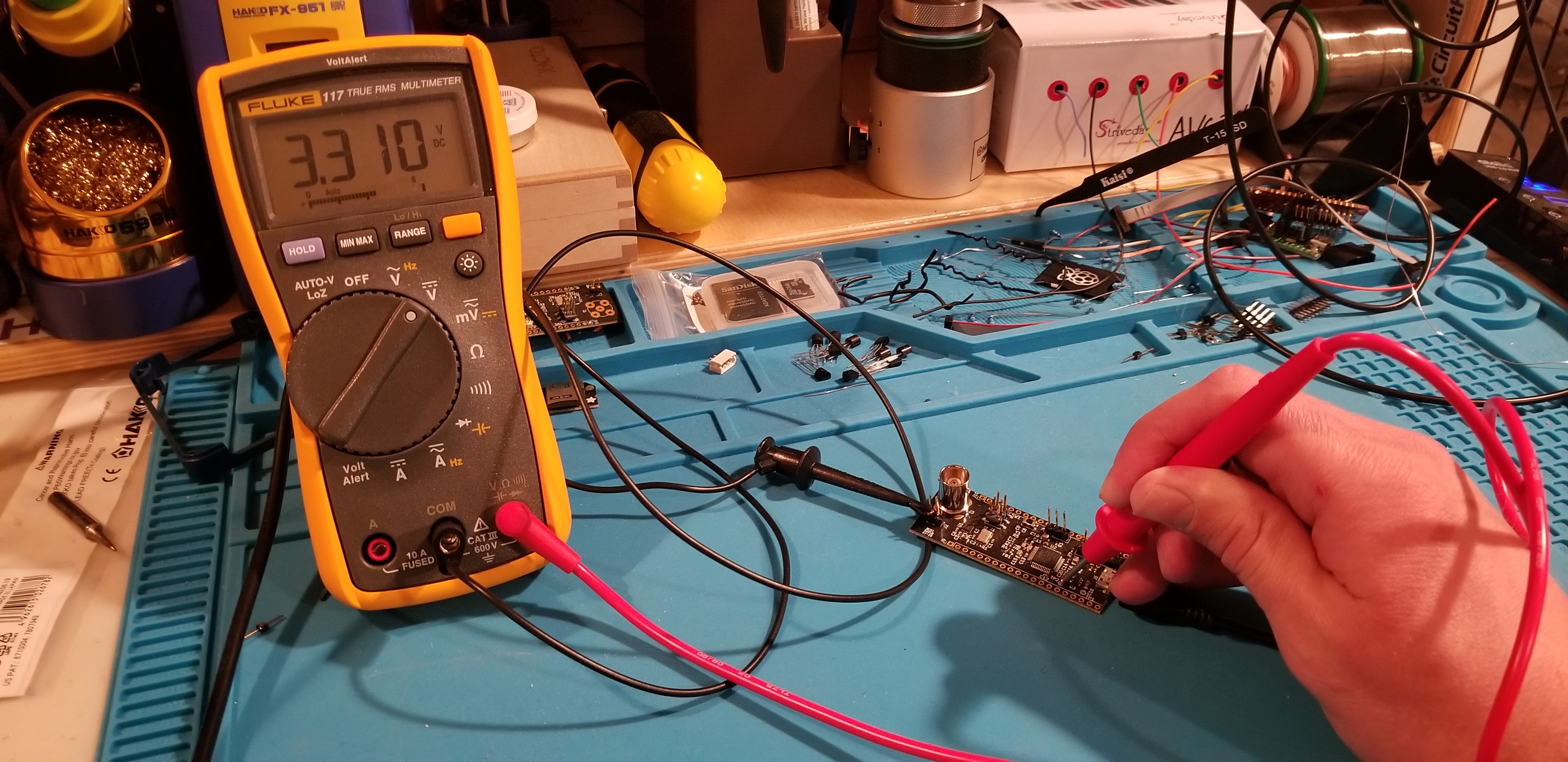
A multimeter is an essential piece of embedded debug equipment. No multimeter is quite as well known as the Fluke handheld 100 series of meters. This is partly by design - their iconic yellow and gray look is trademarked. (For good reason, too!) I particularly love my Fluke 117 handheld meter. It’s a handy tool for all sorts of nuts-and-bolts electrical measurements: current, voltage, DC, AC, autoranging, resistance, capacitance, diode IV ratings, beep for continuity, and a whole host of other features that I can’t think of unless I go dig the manual out of a drawer. What’s not to love?
The Good Parts
A multimeter is a great way to answer all sorts of table stakes questions about your embedded system - for example:
- Is this chip receiving power?
- Are all of the voltage regulators powered?
- Are these two nets shorted?
- Is the reset line asserted/deasserted?
- Is some control line in its proper high/low state?
- How much current is being sunk into my board? (Be careful with this one - beyond 10A, you don’t have a fuse to save you if things get hot!)
- Is my DAC putting out any analog signal at all?
- What’s the quiescent voltage of this ADC input?
Any decent multimeter is capable of this. However, the Fluke models include a wealth of creature comforts that make it a joy to use:
- an “auto off” feature that shuts the meter off after a certain idle period, to conserve battery (I’ve killed many a 9V battery by forgetting to turn off cheaper meters I’ve owned.)
- a backlit display that’s easy to turn on and off at the tap of a button
- a plastic kickstand, so it can stand upright on a tabletop or workbench
- probe clips on the back side of the casing, and a handy soft carrying case
- features for magnetic hanging loops (which I’ve never used but look thrillingly cool if you need to hang your meter from a ferromagnetic rail)
It’s details like this that really elevate Fluke above a generic DMM from Amazon.
The Limitations
While extremely versatile, a multimeter can’t do everything. They are only designed for measuring relatively static signals. You can only get an accurate voltage reading with a multimeter when the target is at a steady state. A toggling GPIO, for example, will show a voltage reading on your meter as a function of its duty cycle. This is because most multimeters are built around a type of integrating data converter called a dual-slope ADC. Dual slope ADCs have several key advantages: they are very robust to component tolerances, easy to auto-zero/auto-calibrate, and consume very little power. What they trade off to do this is bandwidth. Dual slope ADCs are not fast. A relatively pedestrian SAR ADC can take a million samples per second. In contrast, a slope-integrating converter generally cannot exceed a hundred samples per second. This slower speed comes with its own advantages, however: better noise performance, and better notch rejection of unwanted frequencies - particularly those at 50 Hz and 60Hz. If your integrating converter itch isn’t well scratched yet, Maxim Integrated has an excellent tech note describing dual slope ADC theory of operation in great detail.
One last note: the handheld models of multimeter tend to be fairly low precision. You’ll have a hard time measuring anything below 0.01 digits of voltage, current, or resistance. If you need a lower level of detail - say, for measuring precision shunt resistors - a benchtop six digit multimeter from Keithley or similar is a better bet. However, this level of precision is not typically required for garden variety embedded work.
Saleae Logic Analyzer
So, if you’ve got a system driving a lot of toggling IO, and you need to figure out what’s going on, what are you gonna do? Your multimeter, as we’ve just said, isn’t gonna cut it.
An oscilloscope could certainly do the job. You can easily evaluate whether an IO is toggling, and measure time-based parameters like duty cycle and rise time. However, being embedded people, we generally care about interchip communications: things like UART, I2C, and SPI transactions. You can view these on oscilloscopes, but they are painful to decode by hand. Almost all scope vendors offer decoder packages, but they are expensive, and generally not bundled together. You have to pay a few hundred dollars a pop to unlock UART, then SPI, then I2C, and so forth for the smorgasbord of digital signals you need to monitor. On top of that, the UI for many scopes is clunky. Digital protocol decoders can be a pain to configure and steer using only the rudimentary knobs and buttons common to most scope UIs. Remote desktops aren’t much better - these tend to be laggy and difficult to drive.
What you really need is a logic analyzer - one that plays nicely with your development machine.
Fortunately for you, me, and the rest of us embedded folks, this machine exists.
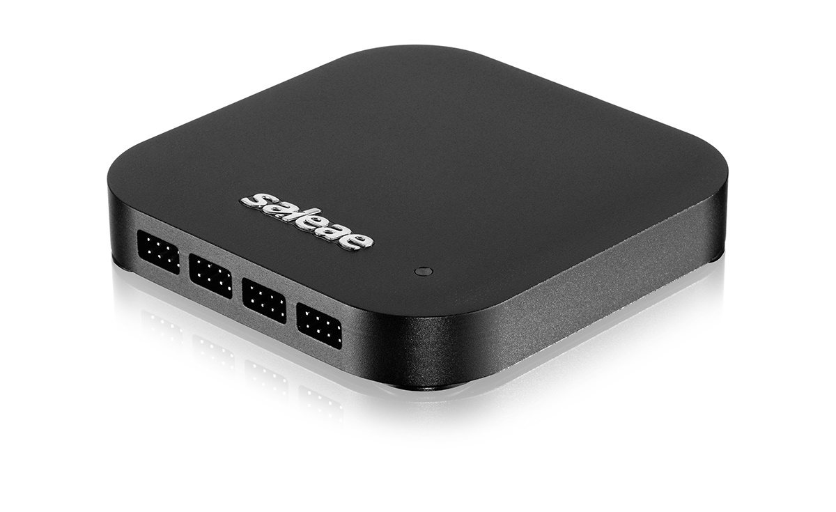
The Saleae Logic Pro16 is, without a doubt, the best logic analyzer on the market for embedded systems.
Logic is the Beginning of Wisdom
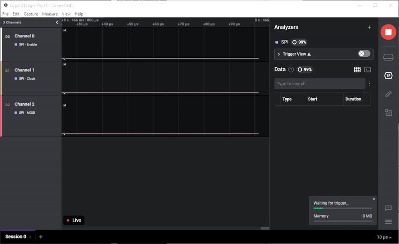
Unlike a scope, where addon decoder packages need to be purchased, protocol analysis is baked into the Saleae by default. The device can decode UART, SPI, and I2C straight out of the box, along with a whole host of other, more obscure protocols. It can handle CAN, 1Wire, I2S, JTAG, SWD, and a whole slew of digital comms with aplomb! It’s also perfectly capable of triggering and reading individual asynchronous IO signals as well. Not sure what you’re looking for on your I2C bus? No problem! Set another IO on your MCU to trigger at a known point in time before the I2C transaction, and the Saleae will do the work of capturing all signals involved.
The Saleae device itself is, quite literally, a black box. (Well, unless you get a pink one like I did.) UI and control happen, instead, through a delightful, easy-to-use GUI. Logic, Saleae’s desktop software, makes it a breeze to navigate logic captures, apply protocol analyzers, and find regions of interest. Scrolling, zooming, and measuring the time between edges is delightful and simple. Surprisingly, this is still true with a touch screen laptop. It was a joy to use a Saleae with my touchscreen-enabled daily driver from a few jobs ago. A big rewrite of Saleae’s firmware and desktop application over the last few years has made the system real-time capable, too!
Saleae also has handy scripting utilities baked into the device. A Socket API with Python and C# bindings allows you to call all sorts of functionality from your favorite programming environment. The Python wrapper even comes with handy command line functionality.
Illogical
The Saleae is a great tool, but it isn’t perfect. It’s only tolerant of low voltage IO signals. Anything between 1.2V and 5V, it can handle with no problems. Use it on higher voltage signals, and you’re gonna have a bad time. It’s also limited to doing relatively low bandwidth digital signals - it caps out at 500MS/s. This is more than adequate for most routine firmware protocols, but for higher speed signals like RGMII, USB3.0, or PCIe, you’re going to need a more specialized piece of equipment.
Additionally - being a logic analyzer, you need to take care that you’re not accidentally degrading the signals you’re monitoring. This can be particularly tricky on faster signal buses, where edge rates of signals are shrinking into single digit nanoseconds. (This author was recently re-educated on this matter by a quad SPI bus running at 30MHz.) All is not lost, though! There are a few relatively simple things you can do to eke out all the signal bandwidth you can out of your Saleae:
- Be sure to include the paired ground test lead when connecting the Saleae to your target board.
- Twist the ground connection together with the signal wire. That way, you’re keeping the impedance of the Saleae’s test leads as low as possible.
- Get rid of the grabber clip if you can. Solder a length of 0.1” header to your target net, and plug the test lead directly to the header.
- Even better: ask your board designer to drop a set of 0.1” headers onto the board. SMT is preferable if you have the space. An SMT header causes less interruption of the ground plane and reduces the chance of causing signal integrity problems due to your debug probe connection.
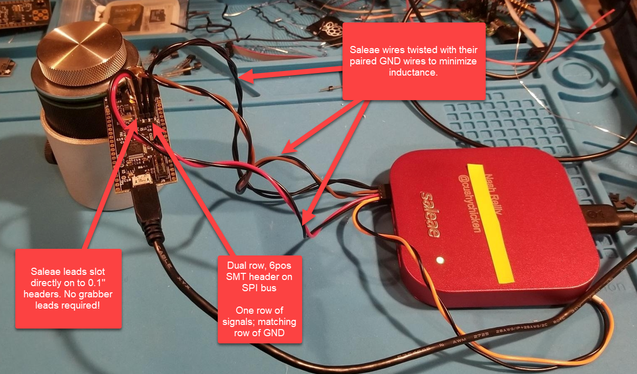
The picture above shows my Logic Pro 16 attached to the SPI bus of a little open source signal generator board I designed in early 2020. It demonstrates the steps you can take to get optimum performance when sampling speedy digital signals with your Saleae.
To me, Saleae is the best of breed in portable logic analyzers. They certainly aren’t the only device of their kind, though! The Digilent Analog Discovery 2, Ian Lesnet’s Bus Pirate, and Great Scott Gadgets’s GreatFET One can all do similar things to the Saleae. These devices also have the advantage of being a lot more affordable than the Logic series, which starts at $479 USD for the Logic 8.
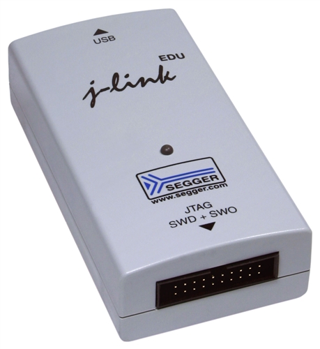
Segger J-Link
What good is a microcontroller if you can’t program it? Segger J-Link debug probes have slowly but surely established themselves as high quality programmers for firmware developers the world over.
Nothin’ but a J Thang
One of the lovely things about J-Links is the multitude of different software interfaces for their probes. Here’s a small sampling of the ways you can chat with your J-Link:
- Command line (J-Link Commander) for daily driver usage
- GDB server interface
- Network interfaces, to allow for JTAG access behind an Ethernet switch
- Factory programmer for speed, verification
- Raw API to write your own
One of the areas in which Segger really shines is their documentation. Segger distinguishes itself with high quality user manuals and application notes. All J-Links come with a 400 page user manual that gives detailed explanations of all functionality in associated software. Much as I love free software, it’s a lovely reminder of how paid software incentivizes you to do a really good job on the hard, not-fun parts of the work, like writing good documentation.
That’s not to say that J-Link doesn’t play nicely with free software! They are more than capable of interfacing with OpenOCD. Sue Mohielden from River Loop Security put together this handy guide showing how to connect to an arbitrary device using a J-Link. According to Sue’s guide, the proper command goes something like this:
sudo ./openocd -s ../tcl -f interface/jlink.cfg -f target/ath79.cfg -c "adapter speed 15000"
Configuring to your specific application is straightforward: simply sub out the
target/ath79.cfg argument for the config file of your target processor. This
can require a bit of rummaging round in the openocd/target install directory
to find the correct file. The exact location of this directory varies from
system to system. Mine is available at the following path on my Linux machine:
/usr/share/openocd/scripts/target. Some trial and error can also be required;
the config files sometimes support multiple processors, while the config file
naming schemes can be somewhat opaque.
This initial configuration process can feel a bit like searching for the proper incantation for a particularly arcane spell. I have struggled with getting OpenOCD working several times. Not to worry! After the umpteenth time of getting grumpy with setup, I took down some notes on how to do it for the next time. I pass it on to you, friends, that your brain sweat be saved for funner problems!
Crash Rules Everything Around Me
Now, back to talking J-Links! The major drawback of the J-Link ecosystem has to be price. The J-Link Base model clocks in at a hefty $450. The Pro Models top out at just under $1200. That is a lot of cash for what is, at the end of the day, a programming tool. However, that price pays for a lot of things that most open source debuggers can’t provide:
- Faster downloading and readback
- Network interfaces
- Real Time Trace - Segger’s fast semihosting/profiling library
Want to tinker around with some of these features, but lack the budget for a full-fledged J-Link? There may be a way for you, the solo developer, to get your hands on their exquisite kit for far cheaper. Segger offers very reasonably priced versions of their probes as the J-Link EDU and J-Link EDU Mini. However, you are prohibited from using them for commercial purposes if you get the EDU models. No cheating! If you’re monetizing your work, you should be ponying up for the Base model at a minimum.
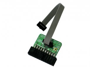
The other minor irk I have with J-Links is their hardware interface. J-Link designs haven’t changed significantly in the decade I’ve been using them. They were, and still are, a fairly stock 20 pin, 0.1” interface. This is a blessing and a curse. On the one hand, it’s easy to wire out the J-Link with 0.1” headers to whatever target device pinout you desire. It’s also easy to hack to better suit your use case - see Jay Carlson’s delightfully clever 3.3V power hack, for example. On the other hand, it means that there’s a whole constellation of adapter boards needed to interface to the multitude of finer-pitched JTAG/SWD connectors. I would recommend, at a minimum, getting something like this Olimex adapter, which changes the 20-pin, 0.1” JTAG interface to the more common 10-pin, 0.05” SWD interface common to many modern dev boards.
FTDI Cable
If there’s an unsung hero of firmware development, it is the humble serial cable. Since the dawn of computing, the UART peripheral has been used as a debug port, a control bus for test systems, and a peripheral interface. It is a ubiquitous communication medium for embedded systems, and for the last two decades, no serial cable has been more ubiquitous than those containing chips by Future Technology Devices International, a.k.a FTDI.
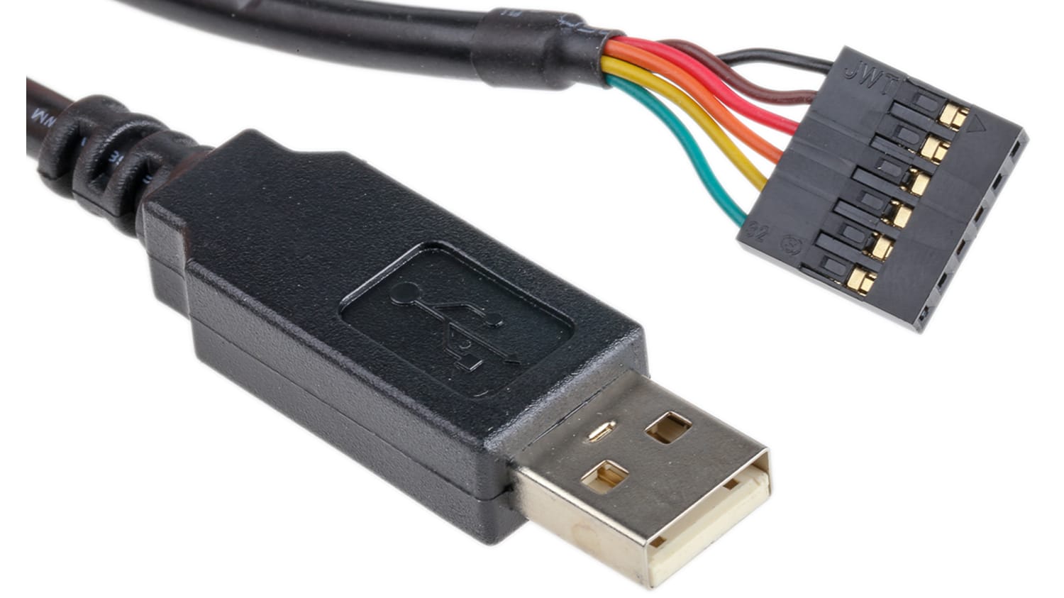
Feeling Talkative, Developer Inquires?
The FTDI TTL-232R-3V3 debug cable is a very common thing to see plugged into a developer machine, or lying tangled on an electronics workbench. Originally a USB device company that made keyboards, joysticks, and mice, FTDI struck gold by creating one of the first cheap, widely available USB-UART interface ICs. It’s an excellent example of a device that does one thing really, really well: it converts USB signals to UART, and vice versa. That’s it! (Here’s a really neat interview Adafruit did with Fred Dart, one of the founders of FTDI. A fascinating look at some semiconductor history!)
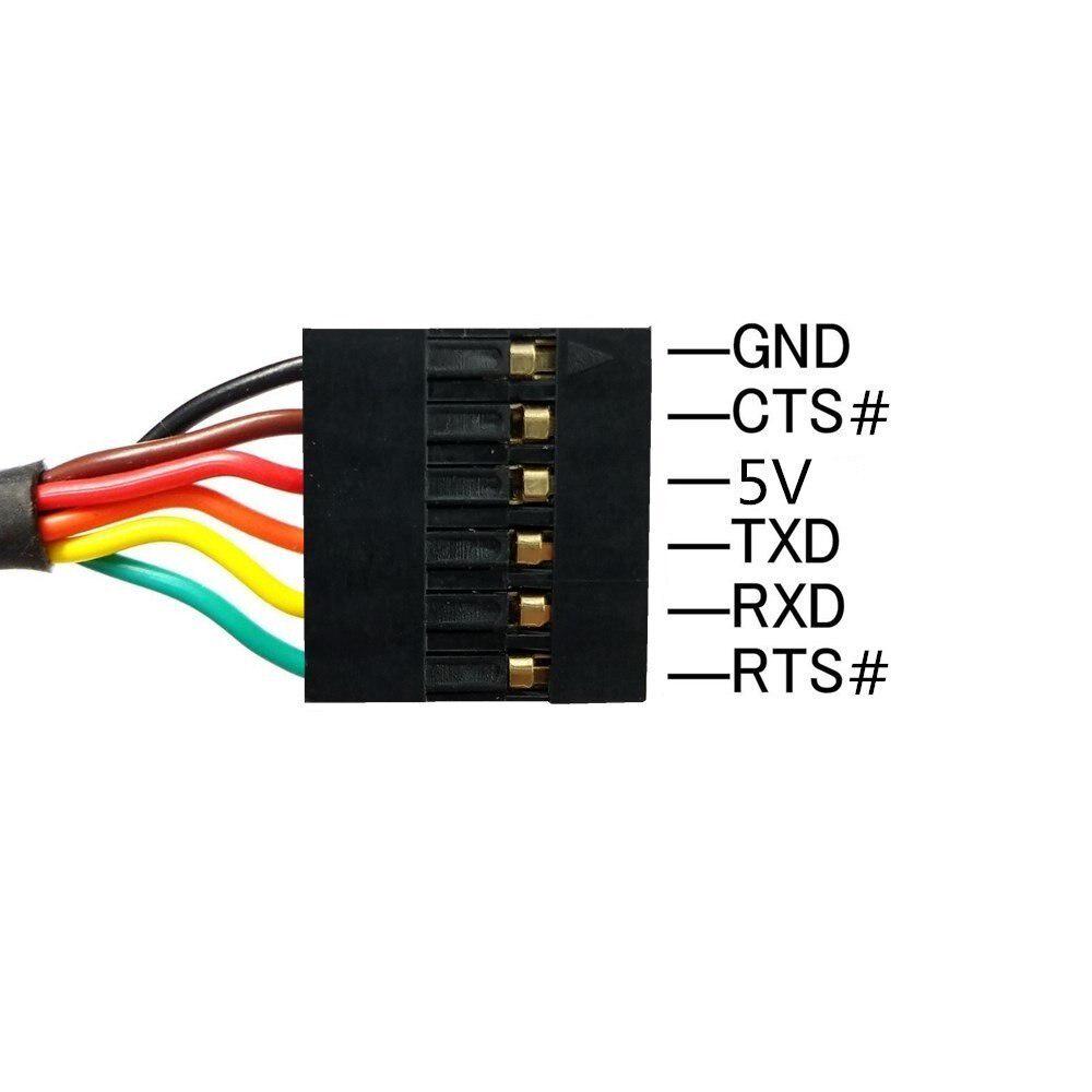
One of the most useful things about the FTDI cable is its ability to provide target power in addition to comms. Each cable exposes a handy 5V output tapped off of the host computer’s 5V USB output. It’s limited at an output of 100mA, but this is more than enough for many bare metal microcontroller applications. A simple on-target LDO stepping down to the proper IO voltage is enough to make this useful to you!
Now Don’t Get It Twisted
If you are responsible for designing PCBs in addition to firmware development, you probably know by now that it is a rite of passage to mix up the TX and RX signals on the FTDI cable, or to reverse the cable pinout. Reversing the pinout is generally a manageable headache. If there’s no mechanical interference, you can typically flip the cable over and be on your merry way. Mixing up the TX and RX signals is a bit more of a headache. However, a set of zero ohm resistors on the TX/RX lines near the connector is generally a good practice. Odds are, you won’t need them - but if you do, it’s a heck of a lot easier than cutting and splicing in a bit of impromptu trace surgery.
Having messed this up myself a time or two, I ended up making a known-good KiCAD schematic containing the proper pinout for the FTDI cable. I also include a little LDO for stepping down to 3.3V, for powering small MCU loads. This is a fairly common SOT-23-5 LDO from Microchip (formerly Micrel); other parts exist in footprint-compatible form factor if you need 2.5V, 1.8V, or lower VDDIO levels. You can find these schematics on GitHub.
I’ve built and tested several designs with this, and have yet to have a headache with it when using it for debugging purposes. I bequeath it to you, that you may never need to splice Rx/Tx between 0402 footprints again!
Conclusion
At the request of the fine folks at Memfault, I’ve been forced to curtail the ode I wrote to my oscilloscope, though I’d be happy to sing you its praises in another post.
What are your favorite tools for debugging firmware? Are there any fun ones I’ve missed? Drop us a comment, or shoot me a tweet (@cushychicken). I’d love to hear about any fun tools you use for your firmware work!
 Nash Reilly works as an independent EE consultant and runs RTLjobs.com, a job site for FPGA and RTL designers. He has previously written firmware for Sonos, Root.ai, and AppHarvest.