Diving into JTAG — Security (Part 6)
The JTAG interface is an important tool for debugging and testing embedded systems, providing low-level access to the internal workings of microcontrollers and other integrated circuits. However, this powerful interface also presents significant security threats. In the sixth and final part of this Diving into JTAG article series, we will focus on security issues related to JTAG and the Debug Port.
Table of Contents
Disclaimer 1: I am not a cyber-security expert and not deeply immersed in this topic, so this article does not aim to uncover any secrets or provide an in-depth exploration. It is a brief discussion from a standard firmware engineering perspective.
Disclaimer 2: This article is for informational purposes only and does not encourage hacking.
Protection
Let’s start by considering simple protection methods that can be applied to make life more difficult for an attacker who wants to gain unauthorized access to a device using the JTAG interface.
Board-Level
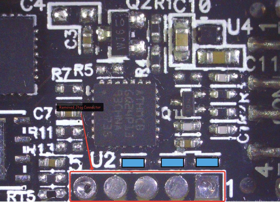
The simplest, most obvious, but probably least effective method of protection is to restrict access to the JTAG connector at the board level. This restriction is achieved by physically removing the JTAG connector from the board at the end of production, as shown in this picture, where you can see that the JTAG connector was removed:
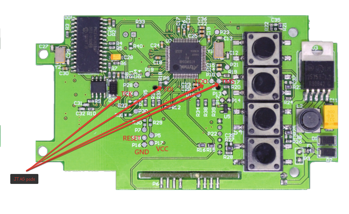
Another protection option is suitable when there is no JTAG connector on the board at all and the JTAG pins are scattered across the board as test points. For example, in the next picture, you can see that the board contains JTAG pins as separate pads.
However, as you well understand, these methods provide only the most basic protection, as soldering a JTAG connector is not a significant effort, nor is finding the necessary JTAG pins on the microcontroller, especially when its part number is written on the package, as shown in the photo. But even if the microcontroller is unknown, there are ways to scan the pins of the microcontroller to discover the necessary JTAG pins (I will discuss these methods in more detail later).
Chip-Level
Debug interfaces are convenient during device development and debugging, but it is good practice to disable them in the release version of the device/firmware. There are configurable bits in the microcontroller’s non-volatile memory to disable certain debug interface functions. The flexibility of configuring protection features depends on the specific core and microcontroller model.
For instance, access to flash memory can be disabled. Some microcontroller models support completely disabling the debug interface. The exact configuration of possible protection features can be found in the microcontroller’s documentation. An example is the Flash Readout Protection (RDP) technology in STM32 microcontrollers. This technology allows for the protection of the contents of the microcontroller’s embedded flash memory from being read through the debug interface.
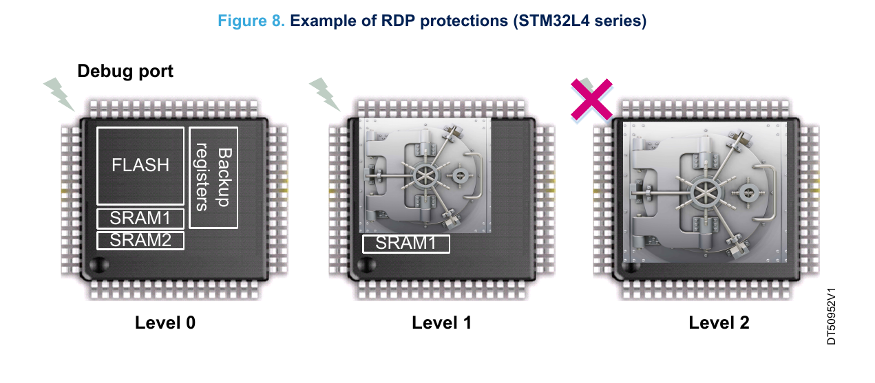
RDP has three levels of protection (0, 1, and 2):
- Level 0 (default RDP level) The flash memory is fully open, and all memory operations are possible in all boot configurations (debug features, boot from RAM, boot from system memory bootloader, boot from flash memory). There is no protection in this configuration mode that is appropriate only for development and debug.
- Level 1 Flash memory accesses (read, erase, program), or SRAM2 accesses via debug features (such as serial-wire or JTAG) are forbidden, even while booting from SRAM or system memory bootloader. In these cases, any read request to the protected region generates a bus error. However, when booting from flash memory, accesses to both flash memory and to SRAM2 (from user code) are allowed.
- Level 2 All protections provided in Level 1 are active, and the MCU is fully protected. The RDP option byte and all other option bytes are frozen and can no longer be modified. The JTAG, SWV (single-wire viewer), ETM, and boundary scan are all disabled.
RDP can always be leveled up. Increasing the level is necessary in the following cases:
-
Intellectual property protection: Increasing the RDP level prevents reading the contents of the flash memory, which protects the firmware and other important data from being copied or analyzed by third parties.
-
Prevention of unauthorized firmware modification: At higher protection levels (e.g., Level 2), it becomes impossible not only to read but also to write to flash memory without completely resetting the microcontroller. This helps prevent the introduction of malicious modifications to the software.
-
Debugging protection: When the RDP level is raised, the microcontroller disables debugging interfaces (e.g., JTAG or SWD), preventing attackers from using them to debug and analyze the program’s operation.
-
Compliance with safety standards: In some applications (e.g., automotive or medical technology), compliance with certain safety standards is required, which necessitates hardware-level data protection.
A level regression is possible with the following consequences:
- Regression from RDP level 1 to RDP level 0 leads to a flash memory mass erase and the erase of SRAM2 and backup registers. You may need to perform a level regression to update software already in flash memory or when you need to repair a production device that has been returned.
- In RDP level 2, no regression is possible.
In consumer products, RDP should always be set to at least level 1. This setting prevents basic attacks through the debug port or bootloader. RDP level 2 is mandatory for implementing applications with a higher level of security.
The RDP technology for STM32 is an example; similar protection technologies exist for other microcontrollers.
Attack
Naturally, if there are defense mechanisms against the use of debugging interfaces, there are also well-known vulnerabilities in these defense mechanisms. Let’s consider the main and most well-known of them.
In general, all attacks can be divided into the following types:
- Software attacks are carried out in particular by exploiting bugs, weaknesses in protocols or untrusted code fragments. Attacks on communication channels (interception or usurpation) fall into this category. Software attacks account for the vast majority of cases. Their cost can be very low. They can be widespread and repeatable with tremendous damage. It is not necessary to have physical access to the device. The attack can be performed remotely.
- Hardware attacks require physical access to the device. The most obvious one uses the debug port if it is not secured. In general, however, hardware attacks are complex and expensive. They are carried out with specialized materials and require electronics skills. There is a distinction between non-invasive attacks (carried out at the board or chip level without destroying the device) and invasive attacks (carried out at the device and silicon level with the destruction of the package).
Attacks on the JTAG interface belong to the hardware non-invasive attack type.
Detecting JTAG pins
If there is absolutely no documentation for a given chip, the first thing an attacker would do is detect the actual JTAG pins. Special tools leverage some features of the JTAG protocol to automate the detection process. Let’s dive into them.
IDCODE Scan
Feature one: very often the IR register is connected to the IDCODE register,
which means that the intended pinout can be tested by a method called IDCODE
Scan. This method is simple because there is no need to scan IR and the
IDCODE register has a fixed length of 32 bits. The algorithm of the method is
as follows:
- First we select the pins we want to scan and put these pins in correspondence
with JTAG lines (
TMS,TCK, etc.), by luck, as you want. But, if there are too many pins to be tested, you can potentially reduce their number by doing some work with measuring the electrical parameters (resistance, voltage) of the tested pins and using these measurements to draw conclusions about the pin belonging to one or another JTAG signal, at least to determine GND and VCC and not to include these pins in further scanning. This procedure is shown very well in this video clip. - Generate the sequence
0b0100on the selectedTMSpin to move to theShift-DRstate. - Hold
TMSin logic zero and generate 32 clock pulses on theTCKpin. - Read the bits to be advanced on
TDO. - If more than one zero or one is read from
TDO, this is a pretty good indication that the electrical JTAG connection is working properly. You can try googling the readIDCODEand with some luck, you will be able to determine not only the JTAG pins, but also the type of microcontroller. If theTDOpin reads only ones or zeros, you have incorrectly assigned the pins in step 1, and you need to reassign the pins and repeat the whole procedure.
However, this method has a number of disadvantages:
- This method does not find the
TDIpin. - If the JTAG circuit contains more than one TAP, it may take more than 32
iterations to find
IDCODE, which means that if after e.g. 64 iterations you do not get aTDOpattern similar toIDCODEon theTDOpin, it does not mean that you have selected the wrong pins; it is possible that the JTAG circuit contains many TAPs.
BYPASS Scan
This method uses the BYPASS register to scan the JTAG circuit. The BYPASS
register allows you to skip a logic element in the circuit and directly transfer
data from input to output, minimizing latency.
- The first step is the same as the first step in the
IDCODEscan method. - Send the sequence
0b01100on the selectedTMSpin to move it to theShift-IRstate. - Send the
BYPASScommand. Since the size of theIRregister is not known, you have to send a large number of ones (as many as 1024, for example). - Send the sequence
0b11000to the selectedTMSpin, thus moving to theShift-DRstate. - Using the
TDIoutput - send some bit pattern that can be easily recognized. - Read the bits from the
TDOpin. If a bit pattern is detected, it means that you have selected the pins correctly.
This algorithm is slower than the previous one, but it can detect all JTAG pins.
If you have a lot of candidate output, it is recommended to first reduce the number of candidates using
IDCODE Scanand then refineBYPASS Scan.
Of course, every time to do all these steps manually is quite boring and tedious so smart people have long ago automated this process. Quite popular tools are: JTAGenum and JTAGULATOR.
If the highest level of RDP 2 protection has been applied to the microcontroller, JTAGulator and similar tools will not help.
Examples of such attacks are described in more detail in the following sources:
- JTAG Scanning
- Hardware Debugging for Reverse Engineers Part 2: JTAG, SSDs and Firmware Extraction
- JTAGulator: Introduction and Demonstration
- 03 - How To Find The JTAG Interface - Hardware Hacking Tutorial
Attack on JTAG
The next thing an attacker will determine is the number of devices in the JTAG
chain, because even if we have only one microcontroller connected to JTAG - the
number of TAPs in the chain may be more than one. Next, we need to determine the
lengths of the IR and DR registers, as well as the number of DR registers
theoretically available.
Determining the number of TAPs in a JTAG chain
The following algorithm can be used to determine the number of TAPs in a JTAG chain:
- Send the sequence
0b01100on theTMSpin, thus switching to theShift-IRstate. - Push a bunch of ones (as many as you can spare, e.g., 1000) through
TDIto allIRregisters in the chain. After this, all TAPs will be inBYPASS. - Send the sequence
0b11000to the selectedTMSpin, thus switching to theShift-DRstate. - Push a bunch of zeros (as many as you can spare, e.g., 1000) through
TDIinto allDRpins in the chain to reset them to zero - Start pushing ones through
TDIintoDR. As soon as you get a one fromTDO, stop. The number of TAPs in the chain is equal to the number of ones pushed in.
Determining the size of IR and DR
The next step is to determine the length of the IR and DR registers:
- Send on the
TMSpin the sequence0b01100thus moving to theShift-IRstate. - Push many ones through
TDIand then send 0. - After that, keep pushing ones to
TDI, counting the number of cycles before 0 appears onTDO. The number of cycles (plus one) will equal the length of theIRregister. - To find the length of
DR, perform the same steps, but in theShift-DRstate
Defining undocumented JTAG instructions
Defining undocumented instructions is useful to an attacker because in many cases, these instructions hide test and debug functions, such as BIT modes for memory and I/O; scan modes; or debug modes and functions.
In the last section, we determined the length of the IR register, and thus we
found out the theoretical number of available JTAG commands (DR registers).
However, the number of actually implemented commands can be much smaller than
the theoretical number. To determine the implemented commands, an attacker must
scan and check the whole range. Fortunately, the IR register is very often
relatively small and unrealized commands usually behave like BYPASS or
generate some fixed value on the TDO pin. However, even with these facts,
identifying undocumented commands is a very difficult task, because the
implementation of commands other than standard commands is not specified in JTAG
and each manufacturer is free to do what it wants, so there is no universal
algorithm, so it is almost always solved by searching all available commands and
trying to determine how the behavior of the microcontroller has changed to
understand what a particular command does.
You can find more details here
Debug Port (RDP) Attack
As we discussed when introducing RDP protection, any device released must have protection enabled. In such cases, to copy the firmware, for example, an attacker has to use techniques such as chip decapping or glitching the hardware logic by manipulating inputs such as power or clock sources and using the resulting behavior to successfully bypass these protections. However, sometimes , an attacker does not have to use such hardcore methods to achieve their goal, especially if the level of protection enabled is not the highest. In this section, I will give a high-level description of a few attack techniques. For a deeper dive, see the full articles linked with each.
Firmware dumping technique for an ARM Cortex-M0 SoC
The first example describes a technique that allows you to read firmware from the nRF51822 device even though memory read protection is enabled. However, the protection level leaves access to the Debug Port and allows the reading and writing of processor registers and even executing debug commands such as step. Through this exposure, an attacker can read the firmware.
Debugger access allows us to write values to the PC (program counter) register
to jump to any instruction and enables us to perform step-by-step execution of
instructions. We can also read and write the contents of the processor’s
general-purpose registers. To read from protected memory, we need to find a
load word instruction with an operand register, set the target address in the
operand register, and execute this single instruction. Since we can’t read flash
memory, we don’t know where the instructions are located. Therefore, it may
sound difficult to find the read word instruction. However, all we need is an
instruction that reads memory from an address in some register to a register,
which is a fairly common operation.
This method is described in detail in the article Firmware dumping technique for an ARM Cortex-M0 SoC. I highly recommend reading it.
nRF52 Debug Resurrection (APPROTECT Bypass)
Here, the situation is more complicated, and the security level prohibits access to Debug Port. Therefore, the previous method will not work.
This is where voltage glitching comes in. Voltage glitching (also known as fault injection or power glitching) is a technique used in hacker attacks on microcontrollers and other embedded systems to disrupt their normal operation and gain access to protected information or functions. This technique is based on temporarily changing (glitching) the power supply voltage of a device, causing it to malfunction. While the microcontroller is running, short bursts (glitches) of low or high voltage are applied at certain points in time that disrupt the normal operation of the device. These glitches can cause errors in the execution of processor instructions, such as skipping or incorrect execution of individual instructions. This can cause the microcontroller to miss important safety checks. If a glitch is successfully synchronized, it can disable security mechanisms or access protected memory, allowing an attacker to retrieve sensitive data or gain control of the system.
The main goal of this method is to find the exact time interval to apply this glitch.
The author of nRF52 Debug Resurrection (APPROTECT Bypass) Part 1 leverages this method by determining the exact time when the AHB-AP has to initialize itself according to the value of the APPROTECT, which is stored in UICR (a dedicated Flash memory partition) and applies the glitch at that exact time, which allows him to bypass the protection and gain access to the DebugPort. I highly suggest reading the original article for a deeper dive on this method.
Conclusion
This article has only scratched the surface of embedded device security in general and JTAG security in particular. If you have experience in cyber security or JTAG attacks, I would love to hear what you have learned and what topics I missed! :) I suggest you read the sources mentioned below – there are so many interesting security discussions there. Well, this article concludes my dive into the topic of JTAG protocol. Thanks to all who read it.
Note: This article was originally published by Aliaksandr on his blog. You can find the original article here.
See anything you'd like to change? Submit a pull request or open an issue on our GitHub
Links
- JTAG Hacking with a Raspberry Pi - Introducing the PiFex
- Hardware Debugging for Reverse Engineers Part 2: JTAG, SSDs and Firmware Extraction
- nRF52 Debug Resurrection (APPROTECT Bypass) Part 1
- nRF52 Debug Resurrection (APPROTECT Bypass) Part 2
- Firmware dumping technique for an ARM Cortex-M0 SoC
- Bypassing CRP on Microcontrollers by Andrew Tierney
- Blackbox JTAG Reverse Engineering
- Glitching and Fault Injection: Re-enabling JTAG on the STM32
- Glitching and Fault Injection: Finding the Right Voltage
- Glitching. A Fault Injection Primer
- Hardware Power Glitch Attack (Fault Injection) - rhme2 Fiesta (FI 100)
- Laser fault attacks | Enter the Donjon
- Power glitch attacks | Enter the Donjon
- Breaking secure hardware with software attacks | Enter the Donjon
- ECED4406 - 0x501 Power Analysis Attacks
- Side Channel Analysis & Cryptography
- Securing the JTAG Interface
- No Code Hardware Hacking - Introducing Glitchy
- SECGlitcher (Part 1) - Reproducible Voltage Glitching on STM32 Microcontrollers
- Backdoor Silicon FUD
- DEFCON 17: An Open JTAG Debugger
- Voltage (VCC) Glitching Raspberry Pi 3 Model B+ with ChipWhisperer-Lite
- Shedding too much Light on a Microcontroller’s Firmware Protection
- Breakthrough silicon scanning discovers backdoor in military chip
 Aliaksandr Kavalchuk is a firmware engineer with over 10 years of experience.