I2C in a Nutshell
I2C is perhaps the most commonly used bus to connect ICs together. As such, firmware engineers encounter it on most projects. In this post, we explain how I2C works, explore common bugs and investigate how to debug these issues.
Table of Contents
Why use I2C
I2C has many advantages:
- It is cheaper to implement than comparable low-power buses, with fewer pins than SPI1, and a simpler physical layer than CAN2 (no differential signalling).
- It supports up to 127 devices on a bus with only two pins.
- It has transfer rates up to 400Kbps, which is fast enough for many human interfaces as well as fan control, temperature sensing and other low-speed contol loops.
- Historically, it has been less onerous for manufacturers to include than competing protocols like Maxim’s 1-wire protocol3.
Many of the sensors and actuators in devices all around us use I2C: temperature sensors, accelerometers, gyroscopes, fans, video bridging chips, GPIO expanders, EEPROMs, …etc.
I2C is not appropriate for all applications however:
- When higher bandwidth is required, SPI may be the right choice and can be found in many NOR-flash chips. MIPI can go even faster, and is often used in displays and cameras.
- If reliability is a must, CAN is the bus of choice. It is found in cars and other vehicles.
- When a single device is on the bus, UART may work just as well.
Anatomy of an I2C transaction
I2C is made up of two signals: a clock (SCL), and a data line (SDA). By default, the lines are pulled high by resistors. To communicate, a device pulls lines low and releases them to let them rise back to high.
Ones and Zeroes
As a digital bus, I2C ultimately transmits 1s and 0s between two circuits. It does so using a very simple scheme: for pulse on the SCL line, one bit is sampled from the SDA line. For this to work properly, the SDA line must remain stable between the leading and falling edge of every SCL pulse. In other word, the value of the SDA line while the SCL line is high is the value of the transmitted bit.
For example, this is 0xC9 over I2C:
Start and Stop
Since an I2C bus may have multiple masters, there must be a way to signal that the bus is in use. This is accomplished with the START and STOP conditions. Every I2C command starts with a START condition and ends with a STOP condition.
To send a START, an I2C master must pull the SDA line low while the SCL line is high. After a START condition, the I2C master must pull the SCL line low and start the clock.
To send a STOP, an I2C master releases the SDA line to high while the SCL line is high.
In the diagram below, we indicate the START and STOP condition with “S” and “P” respectively.
Addresses
I2C is a multi-slave bus, so we must have a way to indicate which slave we would like to send a given command to. This is accomplished with addresses. I2C addresses are 7 bits, a few addresses are reserved and the rest are allocated by the I2C-bus committee. Note that a 10-bit address extension does exist, but is extremely uncommon4.
To communicate with a slave device, an I2C master simply needs to write its 7-bit address on the bus after the START condition. For example, the waveform below captures an I2C transaction to a slave with address 0x66:
Address Conflicts: Since the I2C address space is so limited, address conflicts are not uncommon. For example, you may want to include multiple instances of the same sensor on a single I2C bus.
To enable this use case IC designers typically allow their customers to set a few bits of a device’s I2C address, either by tying pins high or low, or by writing a register. If all else fails, you may use an I2C multiplexer to resolve addressing conflicts.
Reading and Writing
I2C masters may read or write to slave devices. This is indicated with a single
bit transmitted after the address bits. A 1 means the command is a read, and
a 0 means it is a write.
The example below shows a read sent to the slave device at address 0x66.
A common pattern is to send a write followed by a read. For example, many devices expose several registers that can be read/written by first sending the register address to the device in with a write command.
To achieve this, the I2C master must first send a write command with the register address, followed by a second START condition and a full read command (including the slave address).
For example, this is what a write-then-read transaction to read register 0x11
from the slave device at address 0x66 would look like:
Note: I2C does not have a formal way for a slave device to send a command to a master device. Instead, most devices use an additional pin to signal to the master that it should get in touch. Typically, this ends up working like this: the slave device sets that GPIO to high, which raises an interrupt with the master device. The master device then reads a “interrupt source” register which indicates why the slave device raised the interrupt, and goes on to query the device for the information.
Ack/Nack
The I2C protocol specifies that every byte sent must be acknowledged by the
receiver. This is implemented with a single bit: 0 for ACK and 1 for NACK.
At the end of every byte, the transmitter releases the SDA line, and on the
next clock cycle the receiver must pull the line low to acklowledged the byte.
When the line remains high during the next clock cycle, it is considered a NACK. This can mean one of several things:
- A NACK after an address is sent means no slave responded to that address
- A NACK after write data means the slave either did not recognize the command, or that it cannot accept any more data
- A NACK during read data means the master does not want the slave to send any more bytes.
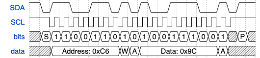
Below is an example of a full I2C write command, with the ACK bits included. It
writes 0x9C to the slave at address 0x66.
Note: A NACK is not necessarily an error condition, it sometimes can be used to end a read. For example, reading 8 bytes from an I2C EEPROM would be implemented by sending a write command to set the EEPROM address offset we want to read from, followed by command which would NACK the 8th byte to signal to the EEPROM device that no more bytes are needed.
Clock Stretching
While control of the SCL line is the domain of the I2C master, an optional feature of the protocol allows slaves to temporarily control it to slow down transmission before it is ready to accept more data.
To stretch the clock, the slave device simply holds the SCL line down. In that state, the master device must wait for the clock rises back up to high before resuming transmission.
This feature is sometimes a source of trouble: not every device supports it, and a master device with no support for clock stretching will hit errors if a slave device attempts to hold the clock down.
Debugging I2C
While I2C is a robust and simple protocol, firmware engineers find themslves debugging unresponsive devices on most projects.
Consider the following scenario: you just received a new board and are doing bringup. You’ve implemented a simple I2C transaction to read the chip ID of a slave device, but are getting back an error (or all 0s).
Let’s walk through what could be going wrong.
Incompatible Devices
The first thing to check is that the master and slave devices are compatible with each other. While I2C is a standard, there are a couple of extensions to it which are not always implemented by every device on the bus.
Specifically, we’ve seen two optional features which can lead to problems:
- 400Kbps bus speed: the original I2C standard specified a bus speed of 100Kbps, but many modern devices support the optional 400Kbps mode. If your master device clocks data in at 400Kbps but your slave only supports 100Kbps, the slave may not respond.
- Clock stretching: clock stretching is an optional feature of the standard, and some slave devices do not support it.
Check your datasheets, and if needed disable optional features on your master device. In doubt, slow the clock down to 100Kbps and disable clock stretching in firmware while configuring your I2C peripheral.
Misconfigured Peripherals
Next, you will want to grab a logic analyzer and probe the SDA and SCL signals. We’re partial to Saleae devices, which come with an easy to set up I2C decoder5.
Looking at a recording of those lines, you should see the SCL line pulse when data is being sent. You can set a trigger on a high to low transition of the clock line if that is easier.
If the line stays permanently low, time to check the pull-ups (see the “Line Pull-Up” section below). If the lines stay high, the I2C peripheral in your MCU is likely misconfigured. Check the code again:
- Are you checking the return value of the I2C initialization and read/write functions? Some peripheral configurations are invalid and will emit errors. For example, a specific I2C peripheral may only be able to map to specific pins. Initializing it with the wrong pins will lead to an error.
- Is your I2C init function being called? Connect your debugger and set a breakpoint in it. Make sure it completes properly.
- Are all the necessary clocks enabled? I2C peripherals rely on specific PLLs or other clocks to generate their signal. Check your silicon vendor’s application notes and make sure you’ve got the right set of peripherals enabled.
If your logic analyzer trace looks like I2C traffic, time to dig deeper into addresses.
I2C Address Issues
Often times, you will see the following on your logic analyzer:
An address is sent on the bus, but it is NACK-ed. Note that NACK is the default state of the lines, so often times it just means: nobody answered.
The first thing to check is: is the address correct? Your logic analyzer will often decode it as a byte, so you will need to shift it down by one bit to recover the 7-bit address. For example, 7-bit address 0x18 would show up as 0x30 in a byte with the lsb set to 0. Check that address against your device’s datasheet.
Some devices have configurable addresses. Check your schematic to make sure configuration pins are pulled up or down as you would expect them.
Last, make sure you do not have address conflicts on your bus. Create a spreadsheet with the addresses of all the devices on the bus, and check for duplicates.
If the address is correct and there are no duplicates, the problem is likely with the slave device. Go to “Slave device disabled or not working”.
Slave device disabled or not working
If the address is correct but the slave device does not ACK it, it is likely not working properly. More often than not, this is because it is not powered or held in reset. Grab your voltmeter and start checking pins:
- Is the power supply of your slave device enabled? You may need to turn on a regulator or toggle a MOSFET.
- Is the chip power the correct voltage?
- Does your slave device have a reset pin? Check that pin and make sure reset is not asserted.
- Does it have an I2C-enable pin? Is that in the correct state?
If all the voltages are correct, test another board or replace the IC. Perhaps an electrostatic discharge damaged your device. If that does not resolve your issue, go to “Line Pull-Up”.
Line Pull-Up
I2C relies on resistors to pull the lines up to the logic HIGH voltage. These resistors may be missing, have too high a resistance, or be connected to a rail at the wrong voltage.
To find it, grab an oscilloscope and probe both the SDA and SCL lines. First, set the oscilloscope in free-running mode and check the voltage:
- If it is consistently 0, pull-up resistors either are missing, or a device is holding the bus low. Check the layout, and verify the pullups are on the board. If they are, start removing I2C devices from the bus by depopulating them until the line rises back to high.
- If it is consistently high, devices are not attempting to communicate over I2C. See the “Misconfigured I2C Peripherals” section.
- Is the voltage correct? Some devices operate at 5V, some at 3.3V, and some even at 1.8V. If a device is expecting a different voltage, it will need to be connected to the bus through a level translator.
If it is toggling, set your oscilloscope to trigger on an edge, and look at the signal. It will likely look like one of these two scope shots shared on StackExchange 6:
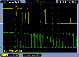
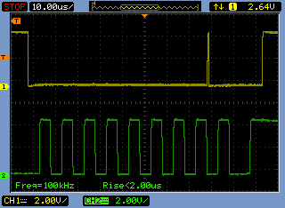
Notice how the second image has sharp, square pulses while the first image has rounded ones? This is your tell. Round pulses are an indications that your pull-ups are too weak. Your logic analyzer might decode them just fine, but an I2C device may have trouble with them.
I2C buses accumulate capacitances when traces are long and devices are added to the bus. You may need stronger pull-ups to overcome it. Counter intuitively, a stronger pull-up is a weaker resistor. In doubt, go to 2K resistors. You will waste a bit of power, but your I2C signal will look great.
Flowchart
To make the process easier, we’ve put together a flowchart summarizing the I2C debugging process. You can find it below, or download it here.

Closing
I hope this post gave you a useful overview of I2C, and how to debug misbehaving buses and devices.
Did I miss any obscure part of the standard, or forget to mention a debugging technique you find particularly useful? Let us know in the discussion area below!
See anything you'd like to change? Submit a pull request or open an issue on our GitHub
Reference
 François Baldassari has worked on the embedded software teams at Sun, Pebble, and Oculus. He is currently the CEO of Memfault.